AFM Systems
AFM Accessories
Learning
Contact Us
 Part of the Oxford Instruments Group
The Semiconductor product development cycle is one of the most intricate and data driven of all industries. As technology nodes continue to shrink below 5nm, Semiconductor manufacturers require the highest resolution, highest throughput, easiest to use equipment to meet technology development and production milestones. One of the most versatile tools for such stringent development requirements is the Atomic Force Microscope (AFM).
Get information from an AFM expertWafer metrology is a vital component of successful Pathfinding and Yield Ramp for the modern Semiconductor Fab. Critical dimensions of <5nm are now becoming common place on bleeding edge technologies, and Semiconductor companies need high repeatability and reproducibility of measurements to ensure proper feedback in the yield learning process flow. The Jupiter XR and Cypher S AFMs from Oxford Instruments Asylum Research offer NIST traceable, closed loop dimension measurements in X,Y, and Z. Patented ultra-low noise LVDT sensors (both Jupiter XR and Cypher S offer <1.5 Angstrom noise in X and Y) provide accurate and repeatable measurements of the smallest critical dimensions.
Ultra flat epitaxial layers are common in semiconductor fabrication. Both Cypher S and Jupiter XR offer <0.35 Angstrom resolution in Z for accurate, repeatable measurements on the flattest epitaxial layers. Read our White Paper "Measuring Surface Roughness with the Asylum Research Jupiter XR Atomic Force Microscope" for more information.
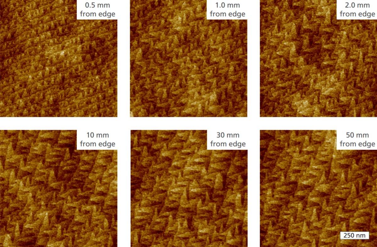
Automated inspection of epitaxial silicon grain structure
Non-uniform grain size can often be observed in epitaxial silicon layers, especially near the wafer edge where there can be greater variations in processing conditions. Here, an automated routine was used to inspect a series of points at different offsets from the wafer edge. The Jupiter software offers flexibility in defining these locations at any point on the 210 mm sample chuck. Roughness (Rq) of each image is only 80-85 pm.
Roughness measurements of a disk media substrate taken 1000 times over 15 hours on Jupiter XR. The Rq roughness remains stable within 1% demonstrating the extreme repeatabiity of Jupiter XR made possible by Asylum's exclusive blueDrive Tapping Mode.
Failure Analysis (FA) and defect characterization in the semiconductor industry has evolved. No longer is it enough to simply analyze returned product. FA processes are being developed to proactively analyze device failure over their lifetime. Additionally, defects and failures that occur in various stages of the production process need to be addressed and looped back into the yield learning flow faster than ever before. An ultra-high resolution, repeatable AFM provides the most detailed and reliable look possible at your devices. AFM provides feedback for both electrical failure analysis and physical failure analysis, as well as tribological, mechanical, and interfacial analysis of devices. We'll look at some FA techniques for semiconductors that involve AFM below.
Nanoprobing, is a method by which nanosharp tungsten probes measure the electrical characteristics and localize defects of integrated circuits. This type of measurement-- typically performed with an AFM nanoprober or SEM nanoprober -- helps semiconductor researchers and engineers test integrated circuits (IC) and other materials during the Yield Ramp and Failure Analysis process. Many of the techniques traditionally performed on a dedicated nanoprobing system can be automated and more cost effectively run on a high speed, ultra-high resolution AFM such as the Jupiter XR or Cypher S. We'll take a look at a couple of the dedicated AFM techniques below:
A technique called Scanning Capacitance Microscopy (SCM), has traditionally allowed for analysis of dopant variations within CMOS devices. Older SCM designs suffered from low throughput and poor sensitivity for lightly doped semiconductors. Oxford Instruments Asylum Research has developed a completely new Scanning Capacitance Microscopy (SCM) architecture that is 20x faster than older designs, and offers 2x more dopant sensitivity for a paradigm shift in SCM performance. In addition to traditional dC/dV amplitude, dC/dV phase differential capacitance measurements, this redesigned SCM module now offers direct capacitance measurements for greatly enhanced dopant sensitivity.
Conductive AFM is another technique which has traditionally been used for rapid Front End of Line defect localization in Semiconductor devices. Previous designs suffered from low dynamic range and only offered a few orders of magnitude current measurement. The Oxford Instruments Asylum Research Dual Gain ORCA CAFM module offers 8 orders of magnitude current resolution (1pA to 10uA) for leaky gate and resistive Drain/Source defect localization in the same image. When coupled with an Ultra-High Resolution AFM such as the Jupiter XR or Cypher S, defect localization on <5nm devices becomes routine. Once defects have been localized, single point I-V curves (current–voltage characteristics) can be obtained from each defect to further analyze the properties of the defect.
To learn more about using Conductive AFM for failure analysis, our webinar "More Than Just Roughness: AFM Technique for Thin Film Analysis" is an excellent resource.
© Oxford Instruments 2024