AFM Systems
AFM Accessories
Learning
Contact Us
 Part of the Oxford Instruments Group


Accelerate your 2D materials discovery and get to your science faster and with ease with our high-performance AFMs. From routinely imaging defects, lattices, and the moiré patterns of twisted van der Waals heterostructures, to precision nanolithography and nanomanipulation, to environmental control, our AFMs offer a complete solution for all your 2D materials characterization needs.
Take your research to the next level and explore novel electronic and quantum phenomena at the frontiers of materials physics with our award-winning, next-generation AFMs.
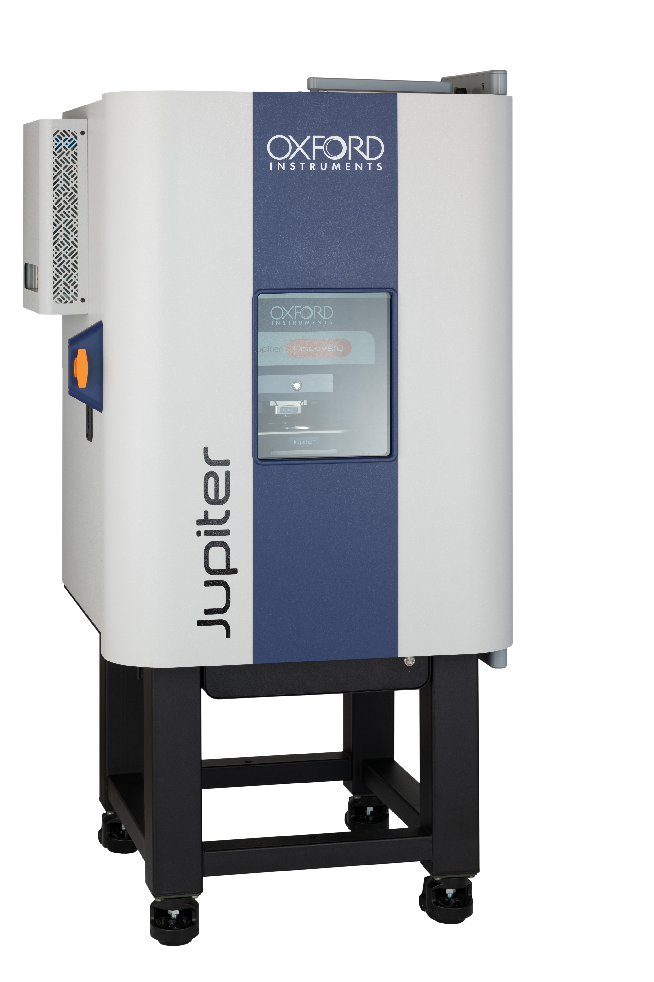
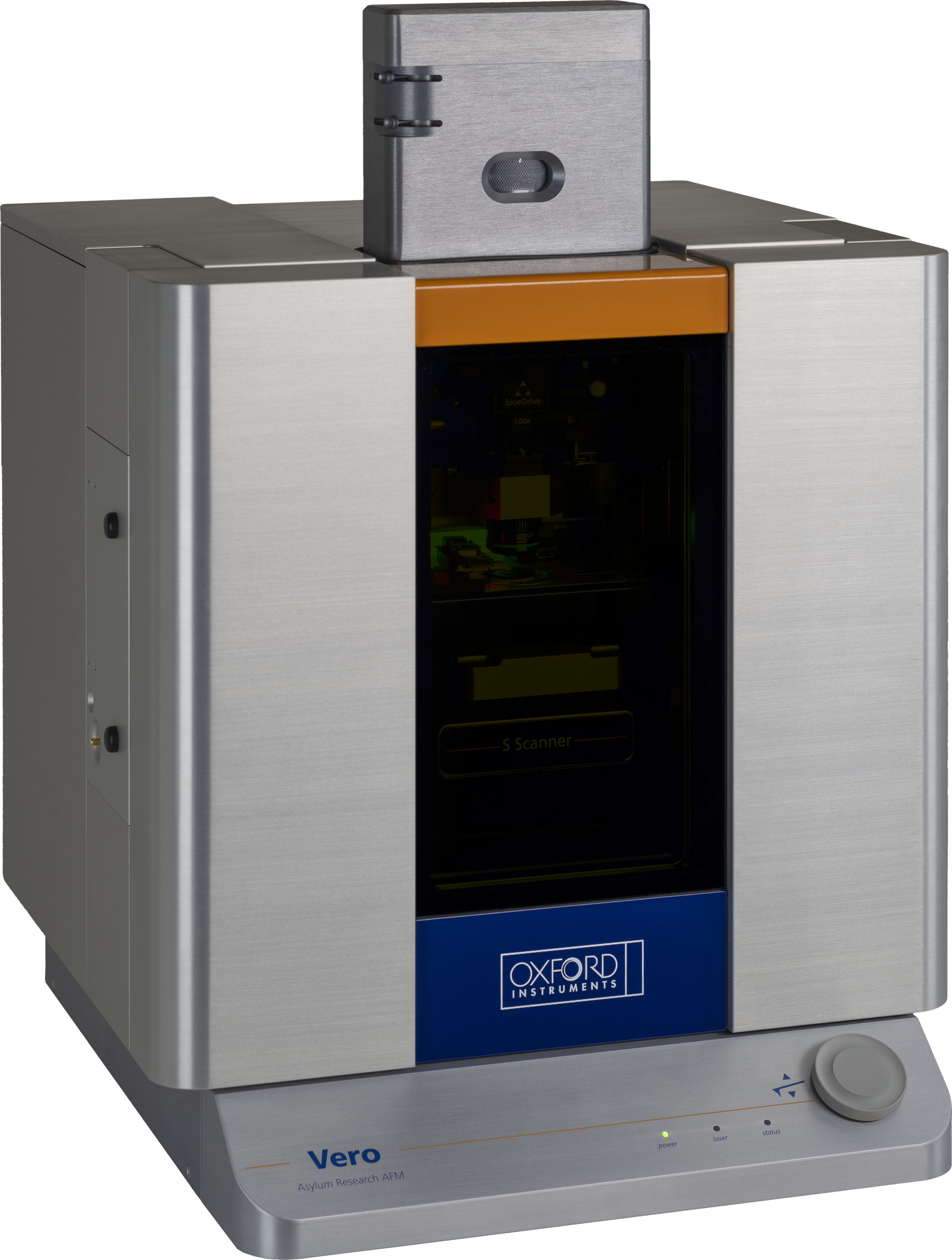
Vero Brochure Jupiter Brochure Cypher Brochure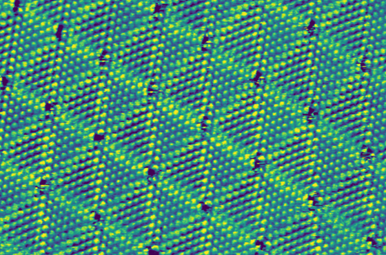
High resolution, one of the hallmarks of our high-performance AFMs, is essential for characterizing twisted van der Waals heterostructures for twistronics, where even fractional changes in the interlayer twist angle can drastically alter material properties. This twist angle can be calculated from the moiré periodicity of the twisted 2D material device. While many AFMs can image this moiré pattern, our AFMs can do this routinely, and quickly - get to your science that much faster and see the difference for yourself.
Torsional Force Microscopy (TFM) is one of several modes that can be used to image the moiré pattern of twisted of 2D materials.
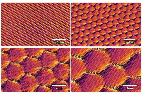
Our next-generation AFMs are designed for high resolution and fast scanning. Compared to conventional AFMs, scanning more than 10x faster enables you to find your region of interest that much sooner.
Closed loop scan control is essential for moiré imaging. Not only does this allow the cantilever tip to be positioned with atomic scale precision, but this also prevents the scan distortion that occurs with open loop scanners.
Accurately measure the moiré periodicity without open loop scan distortion.
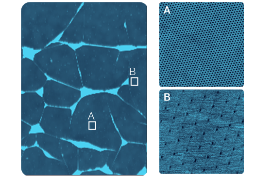
Leading twistronics groups worldwide choose our high-performance AFMs because of how routine it is to image the moiré pattern of twisted 2D materials. Our AFMs' high resolution, fast scanning, and low-noise electronics transform this into an easy task.
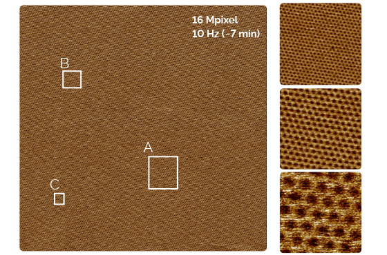
Survey a relatively large area while still preserving the moiré pattern by imaging with megapixel resolution. In this way, you can cover more ground in search of the desired moiré periodicity. This is made possible with our low noise, high speed next-generation AFMs.
Our AFMs set the industry standard for tip-based nanofabrication of 2D materials, delivering the ultimate in precision, reliability, and noise stability required for nanolithography and nanomanipulation. With unmatched force control and precision closed loop positioning, the cantilever tip can reliably cut, slide, and contact clean a variety of 2D materials.
Anodic oxidation lithography enables precise, resist-free nanoscale patterning and cutting of diverse 2D materials like graphene, hBN, and transition metal dichalcogenides. In this mode a biased cantilever tip traces a prescribed pattern that can be imported or drawn manually. All relevant parameters, such as force, speed, frequency, amplitude, and DC bias can be controlled.
The same high-precision force control and closed loop positioning used for AFM imaging enables precise sample manipulation at the nanoscale. Use the cantilever tip to rotate, push, pull, and fold 2D layers, as well as sweep contaminants out of the region of interest.
A MoS₂ flake being rotated on graphene by the AFM tip. Courtesy of M. Liao, Sichuan University.
Go beyond topography with AFM to explore the functional response of your 2D materials. Our comprehensive suite of characterization modes lets you map localized electrical and mechanical properties at the nanoscale.
Explore nanoscale electrical phenomena of your 2D materials with techniques like conductive AFM (cAFM), kelvin probe force microscopy (KPFM), and scanning capacitance microscopy (SCM). These techniques are critical for mapping local variations in electrical properties, as well as delivering multimodal imaging contrast beyond the limits of basic topography.
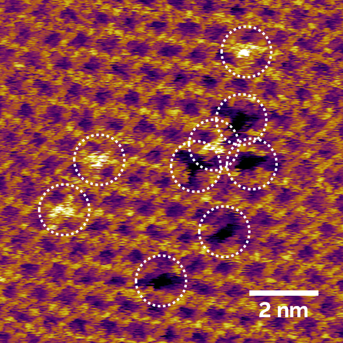
Defects in monolayer WS₂ taken with cAFM. Courtesy of the Velasco and Yan groups, UC Santa Cruz
Advance your 2D materials characterization with our suite of AFM-based nanomechanical modes. These techniques provide quantitative mapping of properties like elastic modulus, viscoelastic properties, adhesion, friction, and mechanical fatigue.
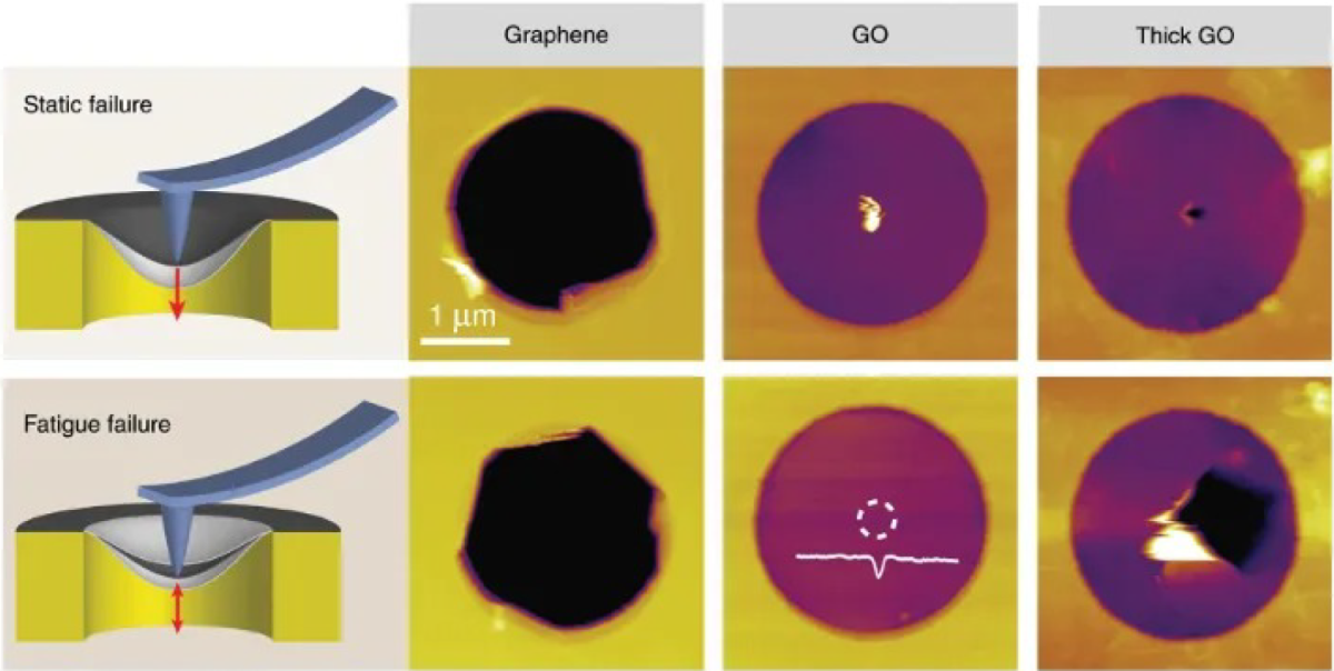
AFM-based fatigue testing of graphene and graphene oxide. Courtesy of T. Cui et al, U of Toronto.
When ambient conditions are not sufficient for your 2D materials research, take control of the sample's environment with our array of options and accessories. Whether you want to prevent sample oxidation with an inert gas environment, track humidity for consistent graphene cutting, or sweep the sample's temperature with high-precision heating and cooling, discover our modular options built to cover your toughest 2D materials research needs.
Typical AFMs struggle with the high vibration and noise levels inside a glovebox. Our high-performance AFMs thrive, routinely resolving the moiré pattern of twisted van der Waals heterostructures, and even achieving atomic resolution without requiring any vibration isolation.
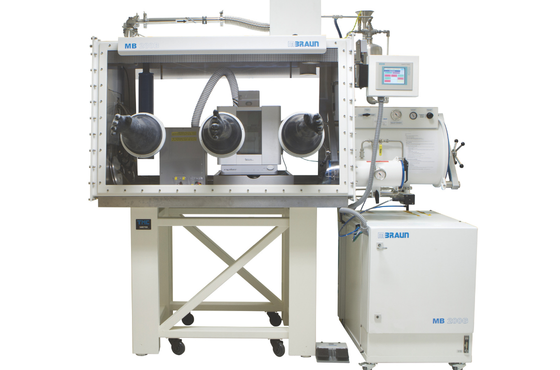
Take control of the environment around your sample with our wide range of environmental accessories.
This tutorial series focuses on the use of atomic force microscopy (AFM) for routine detection and characterization of atomic-scale defects in 2D materials. Traditional approaches, such as scanning tunneling microscopy and scanning transmission electron microscopy, offer exceptional spatial resolution, but can pose challenges in accessibility and practicality for routine measurements, especially those required for process control.

© Oxford Instruments 2026
 Powered by Bioz