For few-layer 2D materials, stacking configuration can be an important degree of freedom for tuning physical properties. For example, trilayer graphene has two stable stacking sequences, ABA and ABC, as illustrated in Figure 1. In the ABA (Bernal) polytype, three individual graphene sheets possess mirror symmetry, resulting in band overlap that imparts semimetallic properties. On the other hand, the ABC (rhombohedral) stacking lacks mirror symmetry and is a semiconductor with a gate-tunable bandgap.
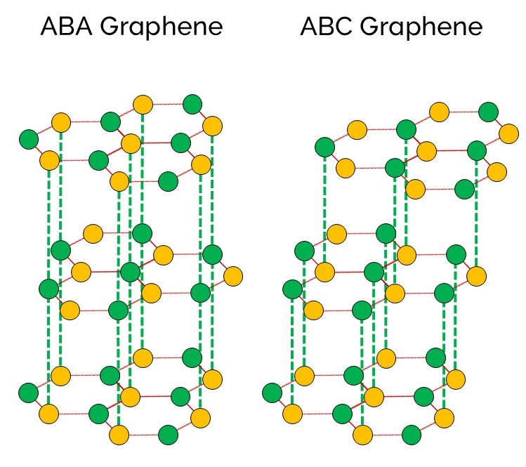
Figure 1: Lattice structure of ABA graphene (left) and ABC graphene (right).
The ABC structure is slightly less stable than the ABA structure and therefore less common on trilayer graphene. It can be prepared by exfoliation, by stacking a monolayer graphene on a bilayer with a small twist angle, or by chemical vapor deposition (CVD) on a curved substrate.1 The unique properties of ABC graphene have attracted significant research interest. Superconductivity,2 insulating behavior,3 and ferromagnetism4 have all been reported on ABC graphene structures.
Research on these graphene systems and other 2D materials requires tools for identifying the stacking order with sufficient spatial resolution. 2D Raman spectroscopy can readily distinguish ABA and ABC graphene domains but is limited by optical diffraction to a lateral resolution of only about 1 µm.5 Infrared Scanning Near-field Optical Microscopy (IR-SNOM) overcomes the diffraction limit by using a sharp tip to collect the local optical signature of samples,6 which enables it to resolve and distinguish trilayer graphene domains (Figure 2b). Though IR-SNOM is non-invasive and high-resolution, it is experimentally complex and is not commonly available as a standard feature on commercial AFMs. In this note, we will demonstrate how Oxford Instruments Asylum Research AFMs can readily and simply distinguish the ABA and ABC configurations using Scanning Kelvin Probe Microscopy (SKPM) and Scanning Capacitance Microscopy (SCM), two nanoelectrical characterization modes available on both Asylum Research Cypher and Jupiter XR AFMs.
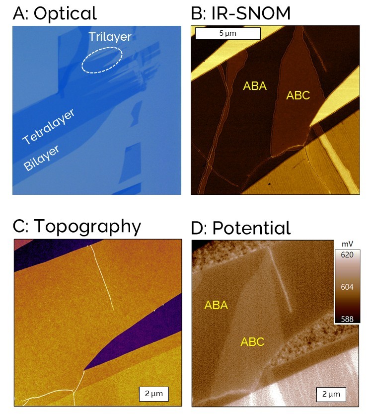
Figure 2: a) Optical image of a graphene flake on a silicon oxide substrate. The trilayer region is located at the top-right area of the flake. b) IR-SNOM image of the trilayer graphene. There is clear contrast between the ABA and ABC domains. c) and d) AFM topography and surface potential image of the same sample with a small lateral offset. Note that the surface potential image clearly distinguishes between the ABA and ABC domains. The IR-SNOM image and graphene sample were kindly provided by Professor Zhiwen Shi from Shanghai Jiao Tong University, China. The SKPM images were taken on a Cypher AFM.
Scanning Kelvin Probe Microscopy, also known as Kelvin Probe Force Microscopy (KPFM), is a standard imaging mode on Asylum Research Cypher and Jupiter AFMs that can measure the surface potential of materials with no special sample preparation. Setup and operation are straightforward and nanoscale surface potential is easily measured with high sensitivity and nanoscale spatial resolution.
It has been reported that ABC graphene has a slightly lower work function than ABA graphene.7 Lower work function leads to a higher surface potential, which can be easily resolved using SKPM. We scanned the same trilayer graphene sample shown in Figure 2b with dual-pass SKPM on a Cypher AFM. There is no contrast between domains in the topography channel (Figure 2c), but as expected, the surface potential of the ABC domain is higher than the ABA domain (Figure 2d). This demonstrates that SKPM can easily and reliably differentiate between ABC and ABA domains with nanometer-scale lateral resolution.
In Figure 3, another trilayer graphene sample is shown as imaged with single-pass SKPM. The layer number (thickness) was confirmed by the AFM topography data. Several ABC domains can be identified in the surface potential image. Figure 3c is a zoomed-in scan of the ABA/ABC domain boundary. Interestingly, there are many small spots with higher surface potential on the ABC domain. An AFM probe in contact mode was then used to sweep that region. As shown in Figure 3d, those materials were removed from the swept area and piled up on the edge of the previous scan area. AM-FM viscoelastic mapping, a nanomechanical characterization mode exclusive to Asylum Research AFMs, revealed that those materials are much softer than the graphene (data not presented here). Therefore, we concluded that they are likely adsorbed organic contamination. In the cleaned region, the measured surface potential of ABC is 13 mV higher than ABA (Figure 3e). This is consistent with a report that their work function difference is in the range of 10-20 meV.7
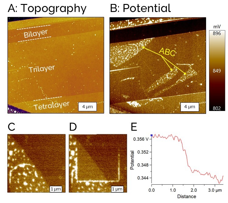
Figure 3: a) and b) AFM topography and surface potential images of a different trilayer graphene sample. c) A zoomed-in surface potential image of the ABA/ABC domain boundary. d) The area in c) was swept by the AFM probe and surface contamination was removed. e) Section line of the surface potential image across the domain boundary. Images were taken on a Cypher AFM.
The band structure of trilayer graphene manifests itself not only in the surface potential but also in electrical conductivity. Conductive AFM (CAFM) is a mode often used for characterizing local conductivity, but it cannot be applied in this case because it requires a conductive sample and here the substrate has an insulating silicon oxide layer. Scanning Capacitance Microscopy (SCM) is another mode that is sensitive to the local impedance of materials. Conventional SCM only works on semiconducting samples that form a native oxide surface layer. However, a new Asylum Research SCM module for Cypher and Jupiter AFMs features much higher sensitivity, which allows the probing of metals and insulators, along with non-linear materials outside the class of traditional semiconductor devices.
Figure 4a shows an IR-SNOM image of a third trilayer graphene sample, where an ABC domain could be identified. Figure 4c is a SCM dC/dV image of the same sample at the location marked with the dashed square in Figure 4a. There is strong contrast between ABA and ABC domains, and the image quality is comparable to IR-SNOM. The Asylum Research SCM module utilizes a ~2 GHz signal to detect the material properties and may be considered as a microwave version of the near-field technique.8 Notice that the ABC domain has shrunk compared to the IR-SNOM result. The SCM test was performed a few weeks after IR-SNOM, and during that time, the domain wall might have moved due to the different thermodynamic stability of ABA and ABC. Figure 4d shows an IRSNOM image of a fourth trilayer graphene sample. Again, the SCM dC/dV image in Figure 4f was able to resolve the small ABC domains. A line section across an ABC stripe shows that the domain width is only about 30 nm at the narrowest location (Figure 4g), demonstrating lateral resolution superior to that achieved by IR-SNOM.
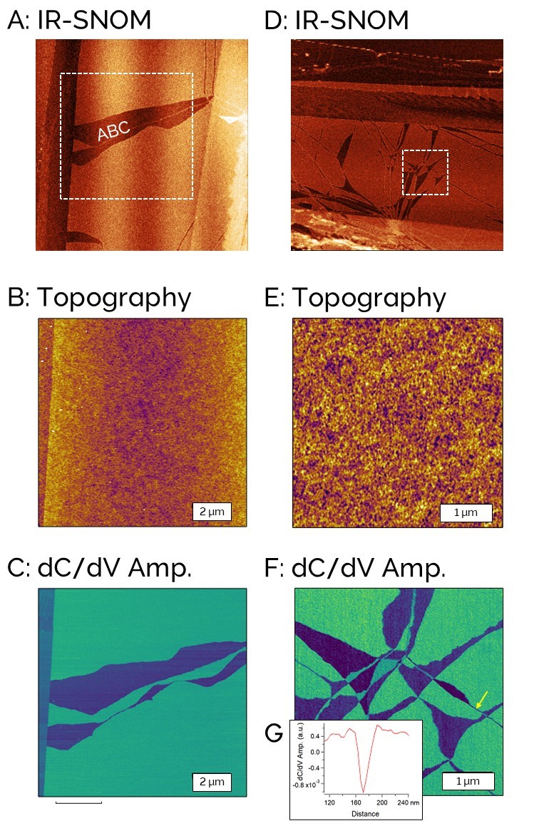
Figure 4: a) IR-SNOM image of a trilayer graphene sample, which shows an ABC domain in the middle. b) and c) Topography and SCM dC/ dV Amplitude images (dotted square area in a). d) IR-SNOM image of another trilayer graphene sample. e) and f) Topography and SCM dC/ dV Amplitude images (dotted square area in d). g) Section line of the dC/dV Amplitude image across a narrow ABC stripe (yellow arrow in f). The IR-SNOM image and the graphene sample were also provided by Professor Zhiwen Shi from Shanghai Jiao Tong University, China. The SCM images were taken on a Cypher AFM .
In summary, we have successfully used both SKPM and SCM to distinguish between ABA- and ABCstacked trilayer graphene. Note that these techniques are not limited to trilayer graphene. They also have excellent potential for characterizing other van der Waals materials with varying stacking structures, such as ABAB- and ABCA-stacked tetralayer graphene and moiré superlattice graphene structures. Both SKPM and SCM offer nanometer-scale lateral resolution that far exceeds diffraction-limited 2D Raman spectroscopy. While IR-SNOM provides another means of distinguishing between these materials at nanoscale resolution, SKPM and SCM are much simpler experimentally and are readily available on both Cypher and Jupiter AFMs. The new Asylum Research SCM module features exceptional sensitivity, which can visualize ABA and ABC domains with stronger contrast and better spatial resolution than both IR-SNOM and SKPM. These results demonstrate that Asylum Research AFMs provide simpler and superior structural characterization of stacked 2D materials.
Characterization of Electrical Transport Behavior in 2D Materials
For fundamental research on 2D materials, structural characterization by AFM is often followed by the measurement of their electrical transport behavior under ultra-low temperatures and high magnetic fields. Oxford Instruments NanoScience provides ultra-low temperature (5 mK) and high magnetic field (up to 20T) environment for fundamental quantum physics research. For example, correlated insulator behavior has been demonstrated on an ABC graphene / hBN moiré superlattice using an Oxford Instruments superconducting magnet cryostat and dilution fridge.4 Visit our Nanoscience colleagues at https://nanoscience.oxinst.com.
References
- Gao, Z. et al. Large-area epitaxial growth of curvature-stabilized ABC trilayer graphene. Nature Communications 11, 546 (2020).
- Chen, G. et al. Signatures of tunable superconductivity in a trilayer graphene moiré superlattice. Nature 572, 215–219 (2019).
- Chen, G. et al. Evidence of a gate-tunable Mott insulator in a trilayer graphene moiré superlattice. Nature Physics 15, 237–241 (2019).
- Chen, G. et al. Tunable correlated Chern insulator and ferromagnetism in a moiré superlattice. Nature 579, 56–61 (2020).
- Lui, C. H. et al. Imaging Stacking Order in Few-Layer Graphene. Nano Lett. 11, 164–169 (2011).
- Ju, L. et al. Topological valley transport at bilayer graphene domain walls. Nature 520, 650–655 (2015).
- Li, H. et al. Global Control of Stacking-Order Phase Transition by Doping and Electric Field in Few-Layer Graphene. Nano Lett. 20, 3106–3112 (2020).

