Since the discovery of the unique properties and exotic physics of graphene, interest in it and other 2D materials and their layered structures has flourished. Graphene has excellent electrical and thermal conductivity, as well as superior mechanical strength. Graphene and other 2D materials have been identified as promising candidates for next-generation transistors in so-called “beyond-CMOS” devices to extend the density and speed of devices beyond current technology scaling limits. However, its lack of an intrinsic band gap limits its utility in such devices. Band gap must be engineered into graphene, for example, by processing it into even lower dimensions (nanoribbons), or by breaking its lattice symmetry by applying strain.1 High-performance atomic force microscopes (AFMs) like the Asylum Research Cypher AFMs offer the necessary resolution and sensitivity to characterize both the structure and electrical properties of 2D materials at the sub-nanometer scale.
Strain can be engineered into graphene, for example, by epitaxial growth.2 When graphene is supported on a substrate that is itself a 2D material, it can generate superlattices called moiré patterns indicating strain from their lattice mismatch. This is the case, for example, when graphene is supported on hexagonal boron nitride (hBN), which complements graphene in device applications as it is electrically insulating. Figure 1 shows moiré patterns directly observed from topographic imaging of graphene layers grown via chemical vapor deposition on an hBN substrate. Note the long-range periodicity observed in the 1-µm scan, and also the short-range periodicity observed in scans below 500 nm, resolved by Asylum’s Cypher S AFM. Moiré patterns are not only visible in AFM topographic images but can also generate interesting physical properties that can be observed with advanced AFM modes. For example, stress induced by lattice mismatch alters the electronic structure of graphene such that moiré patterns can also show up in conductivity, capacitance, piezoresponse and surface potential measurements.
To visualize moiré patterns as well as atomic lattices, the AFMs used for such characterization must be able to detect minute height changes (tens of picometers) and register very low electrical signals. It’s important to note that not all AFMs can achieve atomic-level imaging resolution, which for graphene-based research is important. The word “atomic” in AFM refers to their ability to measure atomic-scale forces, which does not always equate to atomic resolution imaging. Asylum’s Cypher AFM family was specifically developed to achieve industry-leading high resolution performance with a noise floor of just 15 pm, which is at least 50% lower than other commercial AFMs. This requires not only advanced mechanical designs that maximize the rigidity of the mechanical “loop” that connects between the sample and probe but also meticulous optimization of the control electronics to achieve both high bandwidth and low noise. They are also equipped with advanced AFM modes such as conductive AFM (CAFM), scanning capacitance microscopy (SCM), piezoresponse force microscopy (PFM), and Kelvin probe force microscopy (KPFM). These nanoelectrical characterization capabilities are important not just because 2D materials are often incorporated into electrical devices, but also because they can be more sensitive to factors like twist angle, strain, and the number of stacked layers than topographic imaging alone.
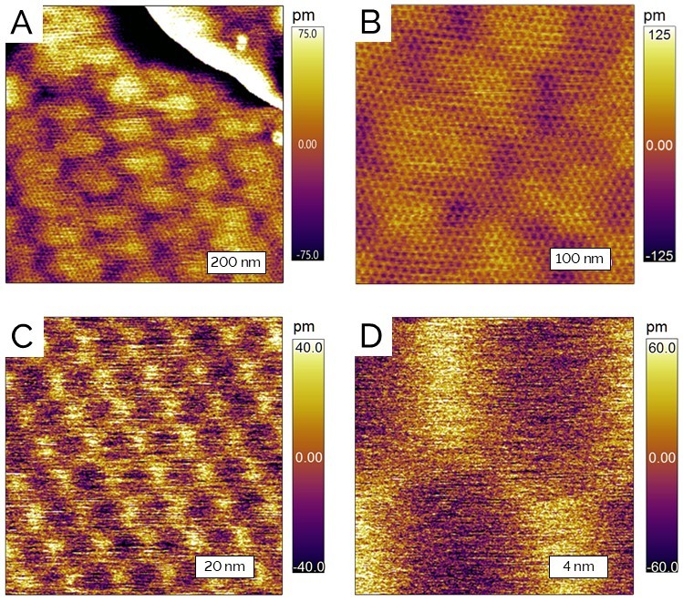
Figure 1: Topographic images of moiré patterns formed by CVD-grown graphene on hydrogen boron nitride substrate.
Graphene can also be stacked into layers held together only by van der Waals forces. Recently, it has been shown that varying the relative rotation (the twist angle) of atomic planes in the stack can have profound effects on the electronic properties of these layered structures.3 Twisted graphene bilayers, for example, are known to form moiré patterns with fascinating electronic behavior; they can either be superconductors or correlated insulators depending on doping. This highly tunable behavior occurs at a narrow range of “magic” angles around 1.1°. These interesting properties depend critically on local stacking configuration, and despite the weak van der Waals interactions between layers, their coupling induces lattice reconstruction in the constituent crystals. This phenomenon has been predicted and observed, for example, in twisted graphene bilayers and in graphene-on-hBN systems.
This note surveys some of the methods available on Oxford Instruments Asylum Research AFMs used to characterize the angle-dependent properties of twisted layers of 2D materials that result from the formation of moiré superlattices.
Resolving Stacking Domains of Moiré Superlattices with Piezoresponse Force Microscopy (PFM) and Kelvin Probe Force Microscopy (KPFM)
Single-layer graphene exhibits interesting physics due to its unique electronic structure making it a zero-gap semiconductor. However, this electronic structure rapidly evolves with the number of layers. Bilayer graphene still approximates a zero-gap semiconductor, but with three layers and beyond, conduction and valence bands begin to overlap. In addition, the relative orientation of the layers gives rise to moiré patterns that modulate the hybridization of the bands resulting in the modification of the band structure depending on the stacking order. Researchers at the University of Washington demonstrated that stacking order produces differences in electronic structure that can be detected via AFM measurements.4 They fabricated twisted double-layer graphene, which consist of two layers of bilayer graphene that are twisted at a small angle. This four-layer graphene stack produces moiré patterns based on two different stacking configurations: Bernal (ABAB) versus rhombohedral (ABCA) stacking, where A, B, and C represent layers that are shifted over the length of one carbon-carbon bond. Bernal stacking exhibits two pairs of low-energy bands, while rhombohedral stacking has only one pair of low-energy flat bands. The moiré patterns result from the lattice relaxing into triangular domains of alternating ABAB and ABCA stacking orders due to atomic reconstruction. These distinctive stacking configurations are predicted to have different transport properties, or a range of correlated and topological states. It is therefore important to characterize the local structure and electronic properties of these moiré patterns.
Moiré superlattices may not necessarily be observed in AFM topography, as Figure 2A shows. However, the AFM tip can simultaneously measure local properties such as piezoelectric strain or surface potential. Figures 2B and 2C show the amplitude and phase of the lateral piezoelectric response on the same area, revealing the triangular ABAB and ABCA stacking domains. Such in-plane electromechanical response has previously been observed via single-frequency PFM on twisted bilayer graphene, which was related to flexoelectricity induced through strain gradients within the moiré superlattices, and regardless of the presence of inversion symmetry in the constituent layers.5 In this measurement mode, an out-of-plane electric field is applied through the tip inducing an in-plane strain response from the sample, whose amplitude is related to the magnitude of the strain, and the phase to the direction of the spontaneous polarization. Single-frequency PFM measurements, however, are notorious for topographic crosstalk, as frequency is sensitive to variations in tip-sample contact, which can obscure the piezoelectric response. DART (Dual Amplitude Resonance Tracking) PFM, a patented technique exclusive to Asylum Research, improves signal-to-noise while eliminating topographic artifacts. Frequency tracking allows the use of enhanced signal from the contact resonance, as well as removing the unwanted effects of frequency shifts due to changing tip-sample contact. This enables the clear distinction between the triangular stacking domains in Figures 2B and 2C. Furthermore, ABAB domains have lower energy than ABCA domains, resulting in the bending of its domain walls into the ABCA domains, as evidenced in the convex shape of ABAB versus concave shape of ABCA domain walls.
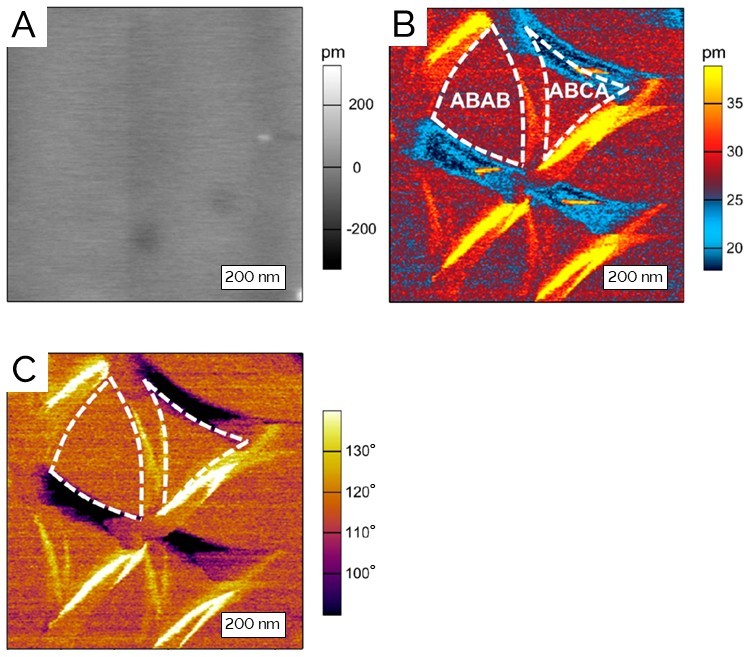
Figure 2: (A) Topographic image of twisted double-layer graphene; (B, C) lateral DART-PFM amplitude and phase images, respectively, showing the ABAB and ABCA stacking domains.
Differences in stacking order which produce differences in electronic structures can also appear as variations in local surface potential within the moiré pattern. Figure 3 shows surface potential maps of twisted double-layer graphene measured by KPFM, where the repeating triangular domain structure in PFM measurements appears here as contrast in local surface potential. Line sections across adjacent domains of different stacking orders show that ABCA domains have slightly higher surface potential (shallower work function) than ABAB domains by about 15 mV. In addition, two types of KPFM measurements were performed: amplitude modulation (AM) versus frequency modulation (FM) KPFM. While AM-KPFM (Figure 3A) is sensitive to capacitance between the tip and sample, FMKPFM (figure 3B) is sensitive to the gradient of the capacitance, and thus more confined to the tip-sample junction, resulting in higher lateral resolution and more accurate surface potential measurements. The two measurements, however, produced similar lateral resolution and magnitude of surface potential, indicating the absence of topographical crosstalk. The difference in surface potential between the two domains observed in KPFM originates from the difference in interlayer hybridization that produces a lower work function with ABCA. Density functional theory calculations indeed show that the two stacking arrangements produce different electronic band structures with ABCA stacking having a higher Fermi energy by about 16 meV.
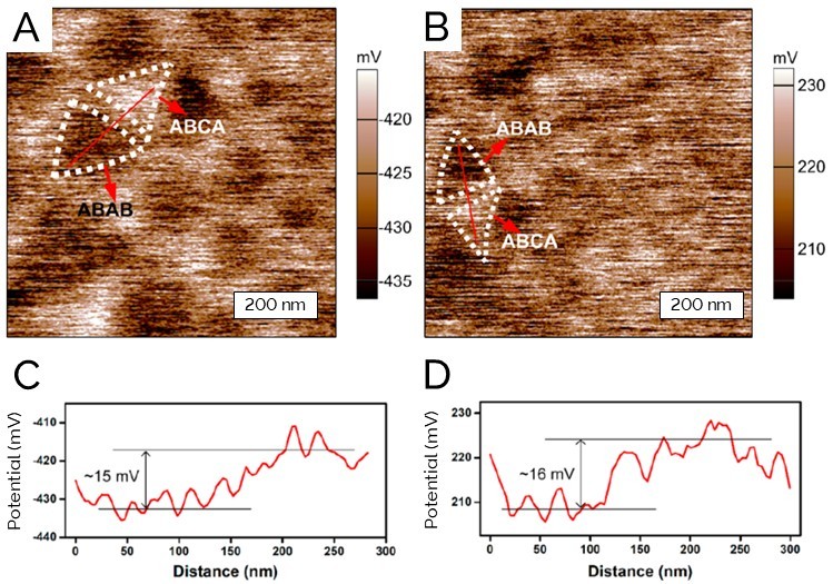
Figure 3: (A, B) AM-KPFM and FM-KPFM images, respectively, of twisted double-layer graphene showing the ABAB and ABCA stacking domains; (C, D) line profiles across the ABAB and ABCA stacking domains showing their surface potential difference.
Characterizing Unusual Low Twist-Angle Conductivity by Conductive AFM (CAFM) and Scanning Tunneling Microscopy (STM)
Twisted bilayer graphene is also found to exhibit unusual conductivity at low twist angles.6 Rotation between adjacent layers produces an incommensurate state that monotonically decreases interlayer conductivity; a phenomena that has been explained by a phonon-mediated interlayer transport mechanism.7 Vertical conductivity (e.g., between a graphene flake and an AFM tip in CAFM mode) also exhibits the same trend. At very low twist-angles, however, competition between interlayer van der Waals interaction and in-plane elasticity can produce local atomic-scale reconstructions that result in moiré patterns with unusual conductivity.
The conductive AFM technique on Asylum Research Cypher AFMs offers significantly higher performance compared to other commercial AFMs. Many CAFM implementations use extremely high gains (e.g. 1012 V/A) and very low bandwidth (~160 Hz) in order to achieve sub-100 fA current resolution. On Cypher, this same current resolution is possible with a gain of only 1010 V/A and a full 1 kHz bandwidth. This enables both significantly faster imaging and a wider current range (<100 fA to 2 nA). The superior noise performance is made possible by a design that places the current amplifier very near the AFM tip and an integrated enclosure around the AFM that acts as a faraday cage to eliminate stray noise interference. This makes Cypher especially well suited for characterizing the conductivity of 2D material structures.
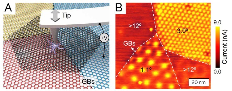
Figure 4: (A) Diagram showing the AFM tip measuring current on twisted bilayer graphenes on hBN with different twist angles generated from a monocrystalline top layer graphene (grey) sitting on a polycrystalline graphene layer (red, blue, and yellow); (B) typical current image measured on domains with different twist angles under a bias of 10 mV.
In this study from Tsinghua University, graphene bilayers were grown on hBN substrates via chemical vapor deposition (CVD).6 This produced single crystal graphene flakes that sit on polycrystalline graphene, which enables a large number of twisted bilayers with varying degrees of twist angles to be interrogated simultaneously (see Figure 4A). Figure 4B shows a typical current image on a graphene bilayer showing domains of different twist angles (1.1°, 3°, and >12°), obtained on a Cypher AFM operating in CAFM mode using the ORCA tip holder with a current amplifier. Four regions with different moiré patterns are clearly resolved, and from the wavelength of the periodicity, the twist angle can be determined. Note that the domain with a 3° twist angle has a higher conductivity than the one with >12°, which is consistent with the expected trend for conductivity with decreasing twist angles. However, contrary to the expected trend, the domain with a 1.1° twist angle has a lower conductivity than the one with 3° twist angle. This unusual drop in conductivity at very low twist angles, revealed by conductive AFM, deviates from previous studies that show a monotonic increase in conductivity with decreasing twist angles.
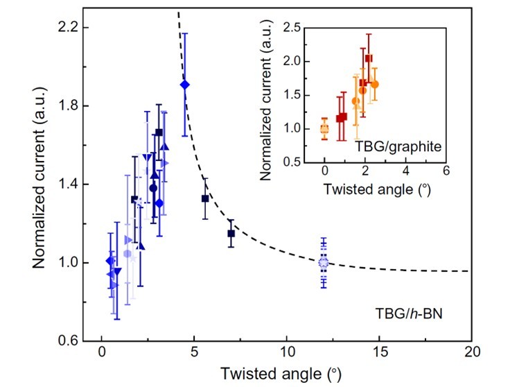
Figure 5: Normalized current versus twist angle of twisted bilayer graphene supported on hBN (main plot) and graphite (inset plot), showing the unexpected non-monotonic decrease of current below 5°.
Figure 5 shows the relationship between the average normalized current and twist angle for a series of graphene flakes. Measurements were normalized against domains with > 12° twist angle to discount systematic variations due to the probe and hBN was also replaced with graphite (inset) to rule out substrate effects. The graph shows that the unusual reduction in conductivity occurs when the twist angle is decreased below ~5°.
Figure 6A shows line sections across normalized current images of bilayer graphene with different twist angles, indicating the correlation of current variations within the domain to the stacking order. Figure 6B and 6C are typical current images showing different moiré superlattice periodicities between domains with 2.9° versus 0.6° twist angles. Regions with higher and lower current within a domain correspond approximately to AB- (or BA-) and AA-stacking regions, respectively. (See Figures 6D-F for schematics of the different atomic configurations for different stacking orders within a domain.) This line section analysis shows that as the twist angle decreases, the current level of AA-stacked regions remains almost the same, while the current level of AB-stacked regions notably decreases. In addition, the areal ratio of the lower current AB-stacked regions increases with the decrease in twist angle from 1.5° to 0.6°. This reduction in the proportion of AB-stacked regions and the isolation of the AA-stacked islands are consistent with local atomic reconstruction unique to low-angle twisted bilayer graphene. These result in the observed decrease in the average current measured in CAFM.
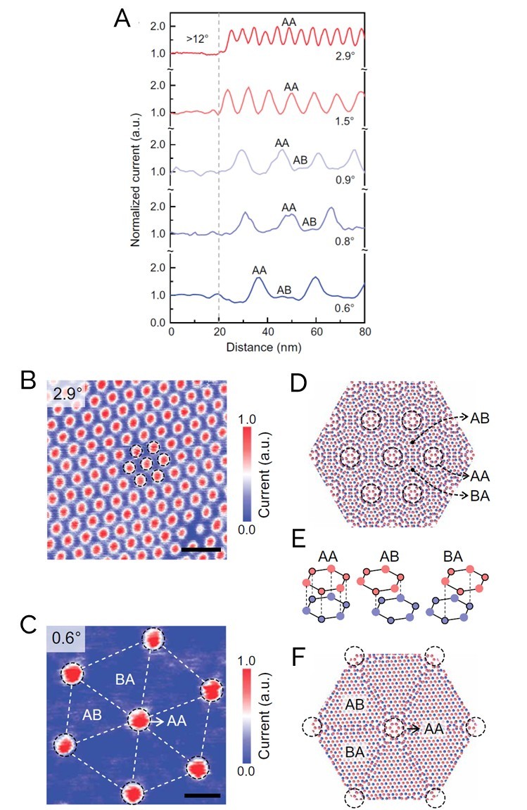
Figure 6: (A) Line profiles of current images at different twist angles, normalized against the current at a domain with a twist angle of 12°; (B, C) typical current images (scale bar, 10 nm) obtained, in this case, at 2.9° and 0.6° twist angles, respectively; (D, F) diagrams showing atomic stacking at these different twist angles, with the AA, AB, and BA stacking regions indicated.
These observations are also confirmed by STM imaging on the Cypher, where moiré patterns with periodicities relating to twist angle were also observed. Contrast in STM, operated in constant current mode, can reflect both the sample topography and density of states; but since the surface was found to be topographically smooth from previous AFM imaging, the contrast here primarily reflects the latter. Therefore, STM imaging demonstrates that the average local density of states decreases with decreasing twist angles.
High-resolution STM can also visualize the sub-moiré lattice structure of graphene in addition to the contours generated by the AB- and AA-stacking orders (Figure 7A). As with AFM imaging, STM imaging on the Cypher platform benefits from its rigid mechanical design and low-noise electronics, which enable it to routinely achieve atomic resolution. Fourier transforms of atomic lattice images from AB-/BA- and AA-stacked regions in a domain with a 1.1° twist angle show a slight orientation difference of 1-2° (Figure 7B). This confirms that the AB-/BA-stacking region locally rotates or reconstructs to form commensurate stacking that gives rise to the unique conductivity of low-angle twisted bilayer graphene.
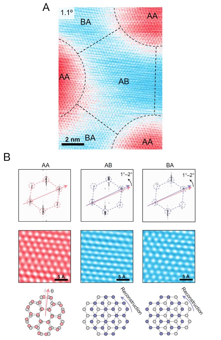
Figure 7: (A) High-resolution STM images (scale bar, 2 nm) of sub-moiré lattice structure measured on a twisted bilayer graphene with a twist angle of 1.1°; (B) Fourier transforms (top row) of atomically resolved images (scale bar, 0.5 nm; FFT-filtered) in the different stacking regions (middle row), and their corresponding diagrams showing the direction of the reconstruction (bottom row).
Note: STM measurements were carried out under a constant-current mode with the same bias voltage of 50 mV
Characterizing the Conductivity of MoS2 Monolayer on Graphene Twisted at Varying Angles Using AFM-Based Nanomanipulation
Transition metal dichalcogenides (TMDs) are another major class of 2D materials that include sulfides, selenides, and tellurides of molybdenum and tungsten. In contrast to graphene, TMDs do have intrinsic band gaps that are highly tunable with strain, pressure, and temperature, which make them promising materials for semiconductor devices. In addition, van der Waals heterostructures of TMDs and graphene also exhibit strong twist angle-dependent vertical conductivities, which was characterized by a group at the Chinese Academy of Sciences.9
In this study MoS2 layers were epitaxially grown on graphene via CVD. AFM topographic imaging confirmed that a monolayer formed from its known thickness. The triangular MoS2 layers exhibited the same hexagonal diffraction pattern as the supporting graphene, indicating that their crystalline orientations are the same: either 0° or 60° twist angles, which are geometrically identical. To change the twist angles between the MoS2 and graphene layers, the AFM tip was used in nanomanipulation mode to physically rotate the MoS2 layer. This was accomplished by landing the tip beside one of the corners of the triangle at a normal load of tens of nanonewtons, followed by moving it laterally across the graphene surface, as shown in the diagram on Figure 8A. By controlling the direction and length of the tip motion, the MoS2 layer can be rotated to any angle. Figures 8B-F show a series of topographic images where the MoS2 layer is rotated sequentially from 0° to 54.4°. Similar nanomanipulation techniques can be employed while applying a high-voltage bias to the tip to cut the graphene into desired shapes or patterns.
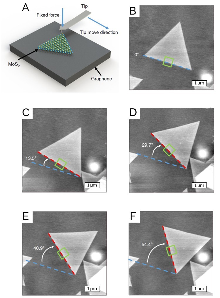
Figure 8: (A) Diagram of AFM tip nanomanipulation setup; (B-F) topographic images of an MoS2 layer rotated on graphene to achieve a series of twist angles.
Note: blue dash lines indicate the original direction of the MoS2 domain, while white arrows indicate the rotation directions; green rectangles represent the scan area during CAFM measurements.
To characterize the angle-dependent conductivity of the MoS2/graphene heterostructure, CAFM was performed, which measures current from the Ohmic contact between the tip and sample, with the sample under bias. Figure 9A shows an FFT-correlated current image of the MoS2 layer with a moiré pattern from the lattice mismatch with the underlying graphene.
In addition, current was measured across the edge of the MoS2 layer (indicated by the green boxes in Figures 8B-F, so that the current measured on MoS2 can be normalized to the current measured on graphene. Figure 9B is a typical current image across the edge showing higher current measured on graphene (i.e., brighter contrast) compared to MoS2 as expected.
Histograms of the current images at different twist angles, normalized to the current on graphene (the peak at 1.000), are plotted in Figure 9C, and shows the current on MoS2 decreasing as the twist angle increases from 0° to ~30°. Figure 9D shows the calculated resistance plotted against the twist angle with an obvious 60° period and a peak resistance at 30°. This demonstrates the highly tunable conductivity of MoS2/graphene heterojunctions by as much as ~5 times with the modulation of their twist angle.
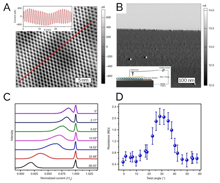
Figure 9: (A) Current image with line profile (inset) showing the moiré superlattice of MoS2/graphene layers (scale bar; FFT-filtered); (B) typical current map across the edge of the MoS2 layer (darker region) with a twist angle of ~28.03° to the bare graphene layer (bright region); (C) normalized current distributions of seven heterojunctions with different twist angle; (D) statistical resistances of MoS2/graphene heterojunctions with different twist angles, with error bars derived from the FWHM of the MoS2 peaks, and each statistic containing at least 20,000 points.
Summary
Layered 2D materials such as graphene, hBN, and TMDs possess interesting electronic properties that can potentially be modulated by varying, for example, their composition and layer order. In addition, the twist angle presents a new powerful parameter for tuning their electrical properties, such as conductivity, piezoelectric response, and surface potential. Despite the weak van der Waals forces between layers, their coupling induces lattice reconstruction in the constituent crystals that produces moiré superlattices whose local stacking configuration, and by extension their electronic structure, depend critically on the twist angle. This application note provides a survey of AFM methods (CAFM, PFM, and KPFM) that can characterize the domain structure of the moiré patterns, as well as the variation in electronic properties with twist angle. Finally, the degree of twist between layers can also be induced by the AFM tip itself in nanomanipulation mode. These examples show how AFMs play a key role in the continuing discovery of novel properties of 2D materials.
References
- Geim, Andre Konstantin. “Graphene: status and prospects.” Science 324, no. 5934 (2009): 1530-1534.
- Summerfield, Alex, Andrew Davies, Tin S. Cheng, Vladimir V. Korolkov, YongJin Cho, Christopher J. Mellor, C. Thomas Foxon et al. “Strain-engineered graphene grown on hexagonal boron nitride by molecular beam epitaxy.” Scientific reports 6, no. 1 (2016): 1-10.
- Cao, Yuan, Valla Fatemi, Shiang Fang, Kenji Watanabe, Takashi Taniguchi, Efthimios Kaxiras, and Pablo Jarillo-Herrero. “Unconventional superconductivity in magic-angle graphene superlattices.” Nature 556, no. 7699 (2018): 43-50.
- Yu, Junxi, Rajiv Giridharagopal, Yuhao Li, Kaichen Xie, Jiangyu Li, Ting Cao, Xiaodong Xu, and David S. Ginger. “Imaging graphene moiré superlattices via scanning Kelvin probe microscopy.” Nano Letters 21, no. 7 (2021): 3280-3286.
- McGilly, Leo J., Alexander Kerelsky, Nathan R. Finney, Konstantin Shapovalov, En-Min Shih, Augusto Ghiotto, Yihang Zeng et al. “Visualization of moiré superlattices.” Nature Nanotechnology 15, no. 7 (2020): 580-584.
- Zhang, Shuai, Aisheng Song, Lingxiu Chen, Chengxin Jiang, Chen Chen, Lei Gao, Yuan Hou et al. “Abnormal conductivity in low-angle twisted bilayer graphene.” Science advances 6, no. 47 (2020): eabc5555.
- Perebeinos, V., J. Tersoff, and Ph Avouris. “Phonon-mediated interlayer conductance in twisted graphene bilayers.” Physical review letters 109, no. 23 (2012): 236604.
- Radisavljevic, Branimir, Aleksandra Radenovic, Jacopo Brivio, Valentina Giacometti, and Andras Kis. “Single-layer MoS2 transistors.” Nature nanotechnology 6, no. 3 (2011): 147-150.
- Liao, Mengzhou, Ze-Wen Wu, Luojun Du, Tingting Zhang, Zheng Wei, Jianqi Zhu, Hua Yu et al. “Twist angle-dependent conductivities across MoS2/ graphene heterojunctions.” Nature communications 9, no. 1 (2018): 1-6.

