AFM Systems
AFM Accessories
Learning
Contact Us
 Part of the Oxford Instruments Group

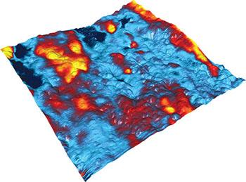
The inherent spatial resolution and direct probing capability of atomic force microscopy make it a powerful tool for nanoscale electrical characterization. Asylum Research offers a full suite of tools for characterizing electrical properties at the nanoscale on the MFP-3D™ and Cypher™ families of atomic force microscopes. While quantitative electrical measurement in itself is the goal, electrical modes are also often used to quickly detect, distinguish, and identify components based on qualitative differences in electric properties relative to other materials in the sample.
Now with the Interferometric Displacement Sensor (IDS) Option for the Cypher AFM, d33 measurements using piezoresponse force microscopy are more reproducible and artifact-free. Interferometric detection directly measures cantilever deflection instead of cantilever angle that is utilized in conventional optical beam detection (OBD). IDS eliminates the artifacts due to electrostatic coupling. Download the data sheet in the white paper tab below.
Ask an AFM expert for more information"Local characterization of mobile charge carriers by two electrical AFM modes: multi-harmonic EFM versus sMIM," L. Lei, R. Xu, S. Ye, X. Wang, K. Xu, S. Hussain, Y. J. Li, Y. Sugawara, L. Xie, W. Ji, and Z. Cheng, J. Phys. Commun. 2, 025013 (2018). https://doi.org/10.1088/2399-6528/aaa85f
"Probing the ionic and electrochemical phenomena during resistive switching of NiO thin films," W. Lu, J. Xiao, L.-M. Wong, S. Wang, and K. Zeng, ACS Appl. Mater. Interfaces 10, 8092 (2018). https://doi.org/10.1021/acsami.7b16188
"Optimization of the Ag/PCBM interface by a rhodamine interlayer to enhance the efficiency and stability of perovskite solar cells," J. Ciro, S. Mesa, J. I. Uribe, M. A. Mejía-Escobar, D. Ramirez, J. F. Montoya, R. Betancur, H.-S. Yoo, N.-G. Park, and F. Jaramillo, Nanoscale 9, 9440 (2017). https://doi.org/10.1039/c7nr01678f
"Spatially resolved multicolor CsPbX3 nanowire heterojunctions via anion exchange," L. Dou, M. Lai, C. S. Kley, Y. Yang, C. G. Bischak, D. Zhang, S. W. Eaton, N. S. Ginsberg, and P. Yang, Proc. Natl. Acad. Sci. U.S.A. 114, 7216 (2017). https://doi.org/10.1073/pnas.1703860114
"New insights on electro-optical response of poly(3,4-ethylenedioxythiophene):poly(styrenesulfonate) film to humidity," E. S. Muckley, C. B. Jacobs, K. Vidal, J. P. Mahalik, R. Kumar, B. G. Sumpter, and I. N. Ivanov, ACS Appl. Mater. Interfaces 9, 15880 (2017). https://doi.org/10.1021/acsami.7b03128
"Mapping the photoresponse of CH3NH3PbI3 hybrid perovskite thin films at the nanoscale," Y. Kutes, Y. Zhou, J. L. Bosse, J. Steffes, N. P. Padture, and B. D. Huey, Nano Lett. 16, 3434 (2016). https://doi.org/10.1021/acs.nanolett.5b04157
"Grain boundary dominated ion migration in polycrystalline organic–inorganic halide perovskite films," Y. Shao, Y. Fang, T. Li, Q. Wang, Q. Dong, Y. Deng, Y. Yuan, H. Wei, M. Wang, A. Gruverman, J. Shield, and J. Huang, Energy Environ. Sci. 9, 1752 (2016). https://doi.org/10.1039/c6ee00413j
"High‐performance and environmentally stable planar heterojunction perovskite solar cells based on a solution‐processed copper‐doped nickel oxide hole‐transporting layer," J. H. Kim, P.‐W. Liang, S. T. Williams, N. Cho, C.-C. Chueh, M. S. Glaz, D. S. Ginger, and A. K.‐Y. Jen, Adv. Mater. 27, 695 (2015). https://doi.org/10.1002/adma.201404189
"Gate-tunable memristive phenomena mediated by grain boundaries in single-layer MoS2," V. K. Sangwan, D. Jariwala, I. S. Kim, K. S. Chen, T. J. Marks, L. J. Lauhon, and M. C. Hersam, Nat. Nanotechnol. 10, 403 (2015). https://doi.org/10.1038/nnano.2015.56
"Polymer homo‐tandem solar cells with best efficiency of 11.3%," H. Zhou, Y. Zhang, C. K. Mai, S. D. Collins, G. C. Bazan, T. Q. Nguyen, and A. J. Heeger, Adv. Mater. 27, 1767 (2015). https://doi.org/10.1002/adma.201404220
"Observation and alteration of surface states of hematite photoelectrodes," C. Du, M. Zhang, J.-W. Jang, Y. Liu, G.-Y. Liu, and D. Wang, J. Phys. Chem. C 118, 17054 (2014). https://doi.org/10.1021/jp5006346
"Solvent‐polarity‐induced active layer morphology control in crystalline diketopyrrolopyrrole‐based low band gap polymer photovoltaics," S. Ferdous, F. Liu, D. Wang, and T.P. Russell, Adv. Energy Mater. 4, 1300834 (2014). https://doi.org/10.1002/aenm.201300834
"Quantifying charge carrier concentration in ZnO thin films by scanning Kelvin probe microscopy," C. Maragliano, S. Lilliu, M. S. Dahlem, M. Chiesa, T. Souier, and M. Stefancich, Sci. Rep. 4, 4203 (2014). https://doi.org/10.1038/srep04203
"A new quantitative experimental approach to investigate single cell adhesion on multifunctional substrates," C. Canale, A. Petrelli, M. Salerno, A. Diaspro, and S. Dante, Biosens. Bioelectron. 48, 172 (2013). http://doi.org/10.1016/j.bios.2013.04.015
"Kelvin probe microscopy and electronic transport measurements in reduced graphene oxide chemical sensors," C. E. Kehayias, S. MacNaughton, S. Sonkusale, and C. Staii, Nanotechnology 24, 245502 (2013). https://doi.org/10.1088/0957-4484/24/24/245502
"High spatial resolution Kelvin probe force microscopy with coaxial probes," K. A. Brown, K. J. Satzinger, and R. M. Westervelt, Nanotechnology 23, 115703 (2012). https://doi.org/10.1088/0957-4484/23/11/115703
"Sub-30 nm scaling and high-speed operation of fully-confined access-devices for 3D crosspoint memory based on mixed-ionic-electronic-conduction (MIEC) materials," K. Virwani, G.W. Burr, R.S. Shenoy, C.T. Rettner, A. Padilla, T. Topuria, P.M. Rice, G. Ho, R.S. King, K. Nguyen, A.N. Bowers, M. Jurich, M. BrightSky, E.A. Joseph, A.J. Kellock, N. Arellano, B.N. Kurdi, and K. Gopalakrishnan Kumar, in IEEE International Electron Devices Meeting 2012 Technical Digest (10-13 December 2012, San Francisco, CA), pp. 2.7.1-2.7.4. https://doi.org/10.1109/iedm.2012.6478967
"Photoinduced degradation studies of organic solar cell materials using Kelvin probe force and conductive scanning force microscopy," E. Sengupta, A. L. Domanski, S. A. Weber, M. B. Untch, H. J. Butt, T. Sauermann, H. J. Egelhaaf, and R. Berger, J. Phys. Chem. C 115, 19994 (2011). https://doi.org/10.1021/jp2048713
"Kelvin force microscopy studies of work function of transparent conducting ZnO:Al electrodes synthesized under varying oxygen pressures," R. Jaramillo and S. Ramanathan, Sol. Energy Mater. Sol. Cells 95, 602 (2011). https://doi.org/10.1016/j.solmat.2010.09.025
"Nanoscale, electrified liquid jets for high-resolution printing of charge," J.-U. Park, S. Lee, S. Unarunotai, Y. Sun, S. Dunham, T. Song, P. M. Ferreira, A. G. Alleyene, U. Paik, and J. A. Rogers, Nano Lett. 10, 584 (2010). https://doi.org/10.1021/nl903495f
"Highly efficient solar cell polymers developed via fine-tuning of structural and electronic properties," Y. Liang, D. Feng, Y. Wu, S.-T. Tsai, G. Li, C. Ray, and L. Yu, J. Am. Chem. Soc. 131, 7792 (2009). https://doi.org/10.1021/ja901545q
"Differential conductivity in self-assembled nanodomains of a diblock copolymer using polystyrene-block-poly(ferrocenylethylmethylsilane)," J. K. Li, S. Zou, D. A. Rider, I. Manners, and G. C. Walker, Adv. Mater. 20, 1989 (2008). https://doi.org/10.1002/adma.200702796
"Space charge limited current measurements on conjugated polymer films using conductive atomic force microscopy," O. G. Reid, K. Munechika, and D. S. Ginger, Nano Lett. 8, 1602 (2008). https://doi.org/10.1021/nl080155l
"Near-static dielectric polarization of individual carbon nanotubes," W. Lu, D. Wang, and L. Chen, Nano Lett. 7, 2729 (2007). https://doi.org/ 10.1021/nl071208m
"Piezoelectric and semiconducting coupled power generating process of a single ZnO belt/wire. A technology for harvesting electricity from the environment," J. Song, J. Zhou, and Z. L. Wang, Nano Lett. 6, 1656 (2006). https://doi.org/10.1021/nl060820v

© Oxford Instruments 2026