Technical Article
2D Materials Create Ultrathin Heat Shields
Author: Asylum Research
Tags: AFM, Atomic Force Microscopy, Kelvin probe force microscopy (KPFM), Scanning Probe Microscopy, scanning thermal microscopy (SThM), SPM
U.S. researchers assembled heterostructures of 2D materials to form thermal isolation barriers for electronics applications. Nanoscale electrical and thermal imaging helped prove these ultrathin heat shields performed better than SiO2 films 100 times thicker.
 Excess heat in laptops, cellphones, and other electronic devices is more than just a nuisance; it can also cause malfunctions and even catastrophic failures. To prevent these problems, most devices contain layers of glass, plastic, or even air that act as thermal insulators. However, such layers can be bulky and hinder efforts to reduce device size.
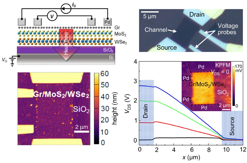
Researchers at Stanford University and the National Institute of Standards and Technology (NIST) have formed ultrathin thermal insulators using 2D materials. Heat shields only 10 atoms thick were created by stacking monolayers of graphene, molybdenum disulfide (MoS2), and tungsten diselenide (WSe2) in various combinations.
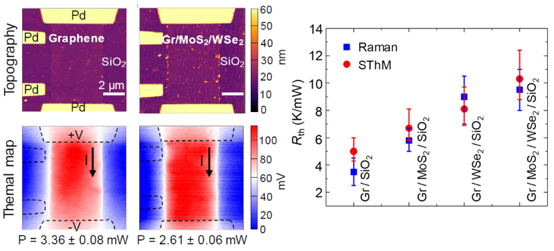
The resulting van der Waals heterostructures had unusually high thermal resistance, meaning they could insulate as well as silica (SiO2) films 100 times thicker. Nanoscale imaging confirmed that the electrical and thermal behavior were spatially uniform across the devices. In addition, Raman thermometry and thermal mapping showed how thermal resistance Rth could be tuned by varying the combination of 2D materials used.
The results demonstrate how to tailor thermal properties at the atomic scale. In this way, they could enable new types of ultracompact electronics and benefit other applications involving heat management.
Instrument used
Techniques used
Images of nanoscale topography and local surface potential were acquired with tapping-mode Kelvin probe force microscopy (KPFM) on an MFP-3D Infinity AFM. Thermal mapping was also performed on the Infinity using scanning thermal microscopy (SThM) techniques and a specialized thermoresistor probe. The results from these diverse experiments highlight the Infinity’s high performance and capabilities for a wide rage of imaging modes.
Citation: S. Vaziri, E. Yalon, M. Rojo et al., Ultrahigh thermal isolation across heterogeneously layered 2D materials. Sci. Adv. 5, eaax1325 (2019). https://doi.org/10.1126/sciadv.aax1325
Note: The original article featured above was published as Open Access under a Creative Commons license. The data shown here are reused under fair use of the original article, which can be accessed through the article link above.