AFM Systems
AFM Accessories
Learning
Contact Us
 Part of the Oxford Instruments Group

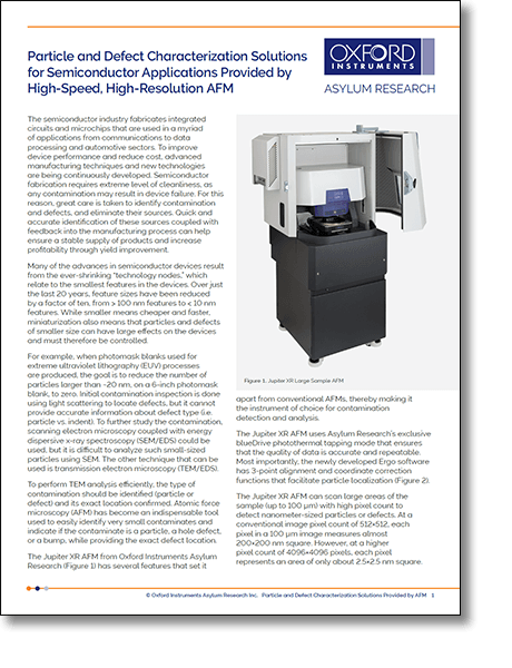
Semiconductor fabrication requires extreme levels of cleanliness, as any contamination may result in device failure. For this reason, great care is taken to identify contamination and defects, and eliminate their sources. Quick and accurate identification of these sources, coupled with feedback into the manufacturing process, can help ensure a stable supply of products and increase profitability through yield improvement.
Download the application note to learn:

© Oxford Instruments 2026