Application Notes
Best Practices for Critical Dimension Measurements by AFM: Probe Selection and Data Analysis
Author: Asylum Research
Tags: AFM, Atomic Force Microscopy
Introduction
Silicon photonics is the study and use of silicon as the optical medium to construct photonic systems such as lasers, detectors, optical communication systems, and more.1,2 Specifically, silicon and SiO2 patterns such as gratings, lines, and sawtooth facets are fabricated on silicon to manipulate light.
Accurate characterization of the shape, size, surface roughness, and surface properties of these patterned structures is critical as they directly impact performance. These measurements therefore can play a crucial role in process development and device optimization. Scanning electron microscopy (SEM) is the most common technique to measure structural feature dimensions, however, it cannot measure other important properties such as surface roughness. Atomic Force Microscopy (AFM) is a non-destructive, mechanical probe-based technique where a sharp tip is scanned over the surface of interest. AFM produces three-dimensional topographic images of the surface with high spatial resolution and can measure critical dimensions and surface roughness (i.e. metrology) as well as detect electrical, mechanical, thermal properties (i.e. material characterization) with little or no sample preparation. This note provides background and guidance for selecting the optimal probes for successful AFM imaging of the critical dimension (CD) features found in silicon photonics.
Critical Dimensions and Surface Roughness
Critical dimensions (CD) are those dimensions that directly affect the function and performance of a device. In silicon photonics, where micro- and nanoscale features manipulate and direct light, any deviation from the design may result in loss of efficiency. Often, these features have high aspect ratios, such as narrow trenches where the depth can exceed the width. Imaging these features accurately can be challenging if the incorrect AFM probes are used.
Surface roughness is another property that is often monitored in silicon photonics because an increase may result in light scattering that can adversely affect device performance. AFM is the only characterization technique that can provide both CD and surface roughness metrology at the length-scales required for silicon photonics applications.
AFM Probe Selection
AFM probes consist of a chip with an attached cantilever that has a very sharp tip fabricated at the end. AFM probes vary in cantilever material and stiffness, as well as in shape, size, and tip sharpness. To image high aspect ratio structures such as diffraction gratings, AFM probe selection is critical. The four key AFM tip parameters that must be considered include: tip length, tip radius, half cone angle, and tip tilt (Figure 1).
To characterize a deep trench structure, for example, the tip must be long enough to reach the bottom of the trench, and the tip radius should be small enough to capture as much bottom width as possible. The half cone angle of the tip must be small enough to fit in the trench top width and capture the (typically) vertical side wall angle. Finally, the tilt of the tip with respect to the cantilever should be adjusted so that the tip contacts the trench feature perpendicularly. This tilt angle is determined by the probe holder geometry which depends on the AFM optics and model.
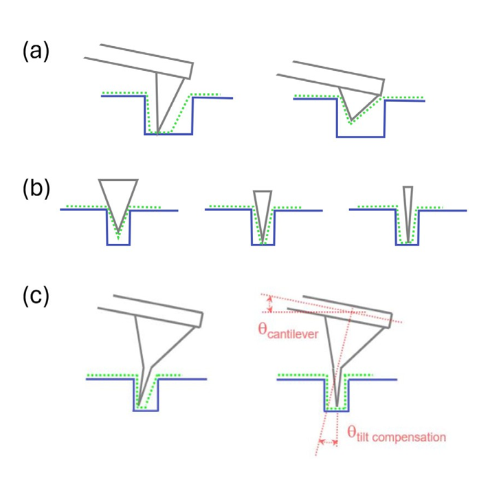
Figure 1: Comparison of AFM probe parameters. Schematics of a scan profile depending on (a) tip length, (b) tip half cone angle, and (c) tip tilt.
Once the relevant feature dimensions are identified, probe specifications based on the four parameters above should be determined and matched with AFM probe manufacturer specs to ensure the most accurate measurements. Note that often no single probe can satisfy the requirements for measuring all the required critical dimensions, and a compromise probe or multiple probe types are required. An example of a good and bad probe choice is provided in the next section.
AFM Characterization of Diffraction Gratings and Waveguides
Silicon/SiO2 diffraction gratings and waveguides were imaged using Jupiter XR AFM and analyzed with AR Maps software. Critical dimensions of the patterned features were obtained from the AFM images and compared with the SEM data provided with the samples. An AFM image of the waveguide pattern and the corresponding analyses are shown in Figure 2. The critical dimensions measured in this example were trench depth and width. AFM data (Figure 2b) was acquired using a standard tapping mode Olympus AC160 AFM probe, which was suitable for imaging this structure because the width of the trenches (~5 um) was very large compared to the depth (~600 nm). AR Maps offers two methods to determine the depth of the trenches from AFM images. The first, as shown in Figure 2c, performs a histogram analysis and calculates the difference between the mean Z-values of the top and bottom planes. In this case, a value of 685.6 nm was obtained.
The second method, as shown in Figure 2d, is a cross sectional height analysis of the AFM image (here averaged over 5 lines) taken orthogonal to the features of interest. In this case a height difference of 686.2 nm was measured in excellent agreement with the first method. However, compared with the SEM data, the AFM depth measurement was greater by about 90 nm. It is possible that the trench depth was underestimated in the SEM data. It is known that SEM images acquired with a tilt can affect distance measurements, and thus accuracy of the results depends on how the SEM image was acquired, e.g., it depends on the angle and position from where the user measured the area of interest. In other words, measurement accuracy is highly user dependent. AFM measurements, on the other hand, measure the vertical position of the tip in perpendicular contact with the sample, and thus the accuracy depends primarily on the Z sensor noise, which is on the order of 30 picometers for the Jupiter XR AFM.
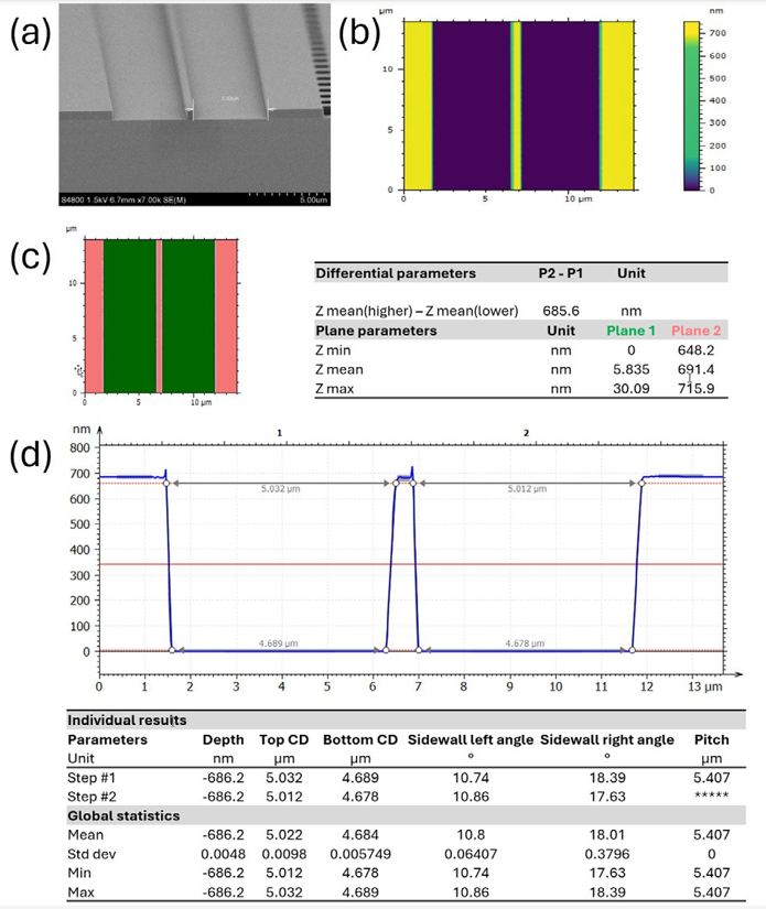
Figure 2. Imaging and analysis of a waveguide. (a) SEM image of the waveguide, (b) AFM image of the waveguide, (c) trench depth measurement by comparison of two planes of the AFM image, (d) trench depth measurement by fitting an averaged cross-section of the data.
Further analysis of the AFM data showed that the top width of the waveguide trench was 5.022 µm and corresponded well with the 5.020 µm measurement by SEM. However, the bottom width of the waveguide trench measured by AFM was only 4.684 µm.
This discrepancy between top and bottom width measurements can be attributed to the shape and half cone angle of the AFM tip. Specifically, the Olympus AC160 AFM probe has a tetrahedral tip shape with a tip angle of 0 degrees and 35 degrees (Figure 3a) side view, and a half cone angle of 18 degrees when looking at the tip head-on (Figure 3b).3
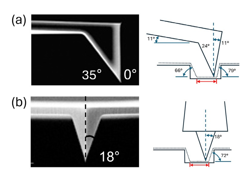
Figure 3. SEM images, schematics of scan profiles, and trench bottom travel for an Olympus AC160 AFM probe. (a) Side view of the probe – when imaging a sample at 0 degrees. (b) Head- on view of the probe – when imaging a sample at 90 degrees. Images are adapted from ref 3.
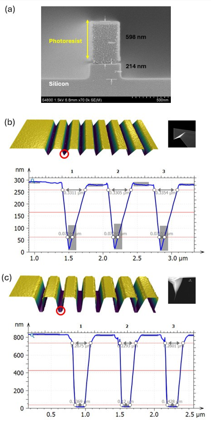
Figure 4. Comparison of AFM data acquired on the same sample using two different AFM probe types. (a) SEM image of the trench sample, (b) 3D AFM image obtained with an Olympus AC160 AFM probe and the corresponding cross-section profile, (c) 3D AFM image obtained with Nanotools NT EBD4-200 probe4 and the corresponding cross-section profile.
Given this tip geometry, the theoretical tip travel at the bottom of the waveguide trench is 4.770 µm. This distance is calculated by subtracting the position of tip-trench bottom contact on the left side, the position of the tip-trench bottom contact on the right side, and the tip diameter, from the trench width. An example of tip geometry, tip angles, and the theoretical tip travel at the bottom of a trench (red arrow) are shown in Figure 3.
The importance of AFM probe selection for characterizing high aspect ratio features is even more evident when comparing results from two different probes measuring the same diffraction grating. An example of such a comparison is shown in Figure 4. The expected depth of the trench is 812 nm, which combines 214 nm of silicon base and 598 nm of photoresist deposited on top (Figure 4a).
Analysis of the topographic image acquired with a standard Olympus AC160 probe (Figure 4b) shows that it was not well matched to the sample features. The AC160 tip is too short and has a large half cone angle which prevents it from reaching the bottom of the trench. The 3D image and the cross-section reflect the triangular shape of the tip rather than the expected rectangular shape of the trench. In contrast, when the same area of the sample was imaged with a specialized high aspect ratio Nanotools EBD4-200 probe (< 5 nm tip radius – 4 µm tip on a 19 µm pyramid), the resulting AFM image was much more consistent with the expected shape of the sample structures (Figure 4c). The 3D image and the associated cross-section analysis showed a flat trench bottom, indicating that the AFM tip did reach the very bottom of the trench, as expected from the 4 µm length of the tip and its small 3 degree half cone angle. The trench depth measured by AFM was 805.5 nm, which was 6.5 nm less than the depth measured by SEM. This depth difference can again be attributed to the difficulty in accurately estimating distances in SEM images, especially if the edges of features are not very sharp, as in Figure 4a. This direct comparison between CD data from two AFM probes on the same area of a sample demonstrates the importance of aligning AFM probe specifications to the specific critical dimension features of interest.
In addition to critical dimension measurements, surface roughness analysis can provide important information for characterizing and optimizing patterned silicon materials. In silicon photonics devices, higher roughness results in increased light scattering, which can decrease device efficiency.5 In the example that follows, the sample is composed of two types of materials: silicon and photoresist. Both surfaces are expected to have low roughness, i.e., (Sq) below 1 nm, with silicon being the smoother of the two.
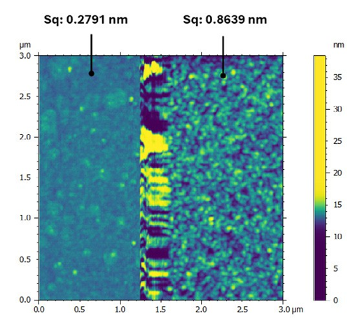 Figure 5. Surface roughness measurement on a sample with both silicon (left) and photoresist (right) surfaces.
The AFM image in Figure 5 was acquired using an Olympus AC55 probe. The image shows both surfaces, silicon (left) and photoresist (right), and is scaled such that the morphology of both regions is visible. Silicon is smoother, as expected, with a roughness (Sq) of 0.2791 nm versus 0.8639 nm for the photoresist. Furthermore, even though the silicon portion of the sample is smoother, it is still not as pristine as expected. The topography shows irregularity in roughness not typical of polished silicon, which is likely due to contamination. In summary, the sharp tip (~7 nm tip radius) of the AC55 probe allows for the characterization of the entire device shape and, is sharp enough to reveal the subtle contamination on the silicon portion of the device. This example shows the advantage of AFM characterization over SEM, as only AFM can provide direct measurements of both critical dimensions and surface roughness data.
Conclusion
Critical dimensions of diffraction gratings and waveguides are most commonly assessed using SEM. However, the capability of SEM to measure other key surface properties is limited. In contrast, AFM provides accurate measurements of critical dimensions, surface roughness, and other surface properties, making it a highly versatile characterization tool for silicon photonics. Despite its advantages, such as the ability to generate high resolution 3D topographic images of surfaces, care must be taken when choosing the best AFM probe for a particular sample. This note illustrates the importance of AFM probe selection on the accuracy of critical dimension measurements through specific examples.
References
- . GT. Reed and A. P. Knights, Silicon photonics: an introduction, John Wiley & Sons, (2004).
- https://photonicsmanufacturing.org/sites/ default/files/documents/front-pdf
- https://probe.olympus-global.com/en/product/ omcl_ac160ts_r3/
- https://nanotools.com/products/blue-line/ ear/ebd4-200a.html
- Sharstniou, S. Niauzorau, A. L. Hardison, M. Puckett, N. Krueger, J. D. Ryckman, and B. Azeredo. Advanced Materials, 34 (43) 2206608 (2022).
If you have any questions about this note please contact AFM.info@oxinst.com
to speak with one of our experts.