AFM Systems
AFM Accessories
Learning
Contact Us
 Part of the Oxford Instruments Group

For those who are newer to Scanning Probe Microscopy (SPM), the term is sometimes treated as a synonym with Atomic Force Microscopy (AFM). But in reality, SPM includes a wider range of techniques where a probe is raster scanned in close proximity to a sample to generate an image. It all started with the invention of Scanning Tunneling Microscopy (STM), for which its inventors, Gerd Binnig and Heinrich Rohrer, were awarded the Nobel Prize in Physics in 1986.
Historically, high-resolution STM imaging was mostly conducted under high-vacuum and cryogenic temperatures. Though STM has been overshadowed in part by AFM in recent years, some of the recent technology innovations at Asylum Research have made it possible to achieve higher resolution with STM, even under ambient conditions. This application note presents examples of low-current STM imaging of self-assembled 2D metalloporphyrin crystals under ambient conditions and demonstrates how molecular resolution can be easily achieved on the Cypher ES SPM.
Download the Application Note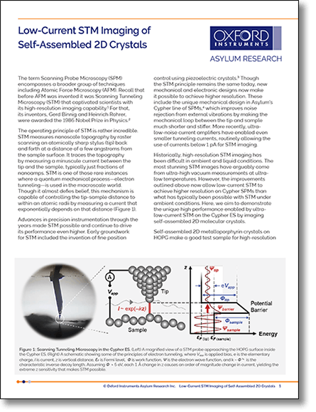

© Oxford Instruments 2026