AFM Systems
AFM Accessories
Learning
Contact Us
 Part of the Oxford Instruments Group
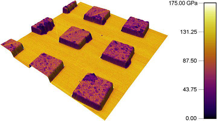
Reference sample consisting of square 200 nm high titanium features patterned on silicon and imaged with Contact Resonance Viscolelastic Mapping mode using blueDrive photothermal excitation on a Cypher S AFM. Shown is the calibrated modulus data overlaid on the 3D topography (Si ~ 165 GPa, Ti ~ 110-125 GPa). Scan size is 25 µm and scan rate was 0.5 Hz. Sample courtesy of Donna Hurley, National Institute of Standards and Technology (NIST).

© Oxford Instruments 2026