AFM Systems
AFM Accessories
Learning
Contact Us
 Part of the Oxford Instruments Group

Graphene and boron nitride
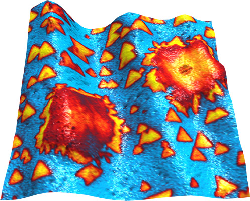
KPFM distinguishes between graphene and boron nitride on a copper substrate
KPFM surface potential overlaid on topography for flakes of boron nitride (triangles) and graphene (circles) grown on a copper foil substrate. At a single atom thick, the flakes cannot be resolved in the topography images due to the roughness of the copper substrate. However, they are readily identified by variations in the SKPM tip-sample potential. The surface potential also distinguishes between the graphene and boron nitride and reveals boron nitride regions growing epitaxially out from the graphene islands. Scan size 60 μm. Imaged on the MFP-3D AFM. Sample courtesy N. Wilson (University of Warwick).
Last Updated: July 12, 2018, 11:13 am
Category: Asylum Gallery Image
