AFM Systems
AFM Accessories
Learning
Contact Us
 Part of the Oxford Instruments Group

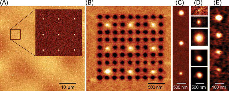
KPFM study on different aspects of charge spot writing for data storage. (A) 25 x 25 array of spots written on a large scale by (5 V / 0.5s) pulses. (B) 9 x 9 array of charge spots (-7 V / 0.5s) with a 3 x 3 array erased by (7 V / 0.5 s) pulses. (C) Spots rewritten by 1, 102, and 104 (-30 V / +30 V, 104 Hz) square wave cycles, from bottom to top. For higher cycling numbers, peak widths are increased. This spot broadening can be reduced by the use of asymmetric pulses of shifted bias or pulse width. (D) From bottom to top: charge spots written in contact with load forces of 1 µN and 10 nN (+30 V / 5 ms), and with lift heights of h = 100 nm, 150 nm, and 200 nm by (+40 V / 10s) pulses. (E) Charge spots written (+15 V, +16 V, +18 V, +20 V / 1s, from bottom to top) and scanned with a high aspect ratio (~7:1) AFM probe. (A,B) on 20 nm PMMA; (C,D) on 40 nm PMMA; (E) on 30 nm COC. Imaged with the MFP-3D AFM.
Date: 16th November 17
Last Updated: July 12, 2018, 11:13 am
Author: Asylum Research
Category: Asylum Gallery Image
