AFM Systems
AFM Accessories
Learning
Contact Us
 Part of the Oxford Instruments Group
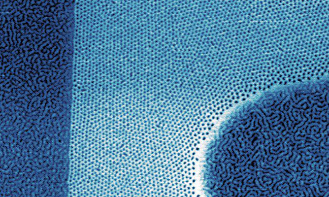
Morphology of PS-PEP diblock copolymer film ? Tapping mode phase image of a polystyrene-block-poly(ethylene-alt-propylene) (PS-PEP) film on a silicon wafer. The darker region on the left side with lower phase corresponds to the high side of a 16 nm step in the wafer. In this region and the darker curved region on the right, the film forms a PS wetting layer. In the lighter region with higher phase, the film contains a single layer of spherical PEP microdomains. Several vertical rows of aligned microdomains are seen on the low side of the step. Diblock copolymers can self assemble into complex periodic structures, a property that has attracted interest for their use as templates in nanolithography. Understanding how film thickness and step height affect domain location and orientation aids in developing block copolymer templates. Imaged with the MFP-3D AFM, scan width 2 µm, Z (phase) scale 10°. Adapted from N.T. Lawrence, J.M. Kehoe, D.B. Hoffman, C. Marks,J.M. Yarbrough, G.M. Atkinson, R.A. Register, M.J. Fasolka, and M.L. Trawick, Macromol. Rapid Comm. 31, 1003 (2010).

© Oxford Instruments 2026