AFM Systems
AFM Accessories
Learning
Contact Us
 Part of the Oxford Instruments Group

Scanning Tunneling Microscopy allows researchers to map a conductive sample’s surface atom by atom with ultra-high resolution, without the use of electron beams or light, and has revealed insights into matter at the atomic level for nearly forty years. This blog post will provide a high-level overview of what scanning tunneling microscopy is, how it works, and how it has been applied in research.
Scanning Tunneling Microscopy, or STM, is an imaging technique used to obtain ultra-high resolution images at the atomic scale, without using light or electron beams. STM was invented in 1981 by two IBM scientists named Gerd Binnig and Heinrich Rohrer. Five years later, the invention earned them the Nobel Prize in Physics.
STM was the first technique developed in the larger class of scanning probe microscopy (SPM) imaging modes. At the time, it allowed researchers to capture significantly more detail than any previous microscopy—all the way down to atoms and inter-atomic spacing. This ultra-high resolution capability allowed researchers to precisely map the three-dimensional topography and electronic density of states of conductive materials, and even manipulate individual atoms on the surface of these materials. Over the following decades, STM has revolutionized the field of nanotechnology and continues to play an important role in fundamental and industrial research across a variety of disciplines.
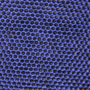
STM image of highly-oriented pyrolytic graphite (HOPG)
Acquired in air on an Asylum Research Cypher S scanning probe microscope, demonstrating the ability to resolve the atomic lattice structure. (5 nm scan size)
STM is a remarkable and rare example of harnessing a quantum mechanical process (electron tunneling) in a real-world practical application. The term “tunneling” refers to the situation where electrons traverse a barrier (in this case, a tiny gap between the tip and surface) that initially seems like it should be impenetrable—like throwing a ball against a wall. The physics that describes this ball-wall interaction is called the “classical paradigm,” and the ball will never tunnel through the wall. Electrons, by contrast, have a quirky wave-like character that makes them a “fuzzy” cloud (unlike a ball), so they can actually exist on both sides of the barrier simultaneously and therefore have a non-zero probability of moving across the barrier even if the barrier energy is higher than the total energy of the electron.
STM works by scanning a sharp conductive probe very close to the surface of a conductive specimen and forcing electrons to traverse the gap between them. When the tip is sufficiently near the surface (usually <1 nm away), the fuzzy electron cloud of the first atom of the tip and surface begin to overlap. Applying a bias voltage between the tip and the surface in this configuration produces a current because electrons are driven to tunnel through the potential barrier from the tip to the surface via the overlapping electron cloud. This tunneling current is highly sensitive to the gap between the probe tip and surface, varying exponentially with the tip-sample distance. As the tip scans line by line across the surface of the sample, the intensity of the tunneling current maps the sample’s electronic density of states.
The STM operates in two distinct modes: constant height mode and constant current mode. Constant height mode is generally used when the sample surface is very smooth. In this mode, the probe tip stays at a set height while it quickly raster scans across the sample. By measuring changes in the intensity of the tunneling current as a function of (x,y) position and bias voltage, researchers can construct an image of the electronic density of states of the sample surface, defects, frontier molecular orbitals, and more.
The more popular mode is known as the constant current mode. In this mode, the tunneling current is held constant by the use of a feedback loop system that adjusts the distance between the tip and the surface. That is to say, if the tunneling current exceeds the target value, the feedback control system will increase the distance between the tip and the sample; if the tunneling current is less than the target current value, the feedback control system will bring the tip closer to the surface of the sample. The resulting three-dimensional distance profile as a function of (x,y) position can help researchers measure a wide array of characteristics, including surface roughness, defects, and the size and conformation of molecules on the surface.
STM can operate under a wide range of different environmental conditions. Often, STMs are categorized as either ambient STMs or ultra-high vacuum (UHV) STMs. Ambient STMs typically operate in air or other gases at near room temperature. With specialized insulated tips, ambient AFMs can also be operated in liquids. Oxford Instruments Asylum Research offers ambient STM capabilities on both our MFP-3D SPMs and Cypher SPMs.
UHV STMs differ, obviously, in that they operate under very high vacuum. This is often done in highly specialized UHV systems where the sample is grown or etched and then imaged in situ. Their operation in vacuum allows them to operate across a very wide temperature range, from near zero Kelvin to over 1000°C. Asylum Research does not offer UHV STMs, though the Oxford Instruments Nanoscience group produces UHV equipment sometimes used with STM.
Since its discovery, the STM has been responsible for major breakthroughs in nanotechnology and has enabled novel research across various disciplines, including semiconductor science, electrochemistry, surface chemistry, and more.
Initially, the STM was used to characterize the topology of different metals and delineate the atomic structure of their surfaces. For the first time, researchers were able to discern the atomic-scale properties of materials, including surface roughness, defects, and surface reaction mechanisms. By investigating the atomic lattices of materials, researchers could begin to understand properties relevant to the fabrication of electronic components, including conductivity, distributions of frontier molecular orbitals and their energies, and reaction dependencies on crystal facet orientations, to name a few.
Over the years, STM began to be employed for a variety of applications outside of atomic-scale imaging. It has been used to assemble and manipulate individual atoms on a surface. This opened up new vistas for nanotechnology, including the generation of nanostructures such as quantum corrals and molecular switches. Contacts on nanodevices can also be constructed with STM by depositing metals (such as gold, silver, or tungsten) in a specified pattern. Researchers have also used STM to induce chemical reactions and study the subsequent reaction mechanisms at the molecular level.
Ambient STMs are commonly used to investigate the structure of self-assembled molecules on surfaces because they can often resolve single molecules and even sub-molecular structure. For example, the image below clearly shows single molecules of 5-octadecoxyisophthalic acid in a self-assembled monolayer on HOPG.
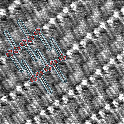
STM image of a self-assembled monolayer of 5-octadecoxyisophthalic acid on highly-oriented pyrolytic graphite.
Molecular models are overlaid to emphasize the molecular ordering. Imaged on a Cypher AFM, 15 nm scan. Sample courtesy of Matt Blunt, University of Nottingham.
More recently, low-current STM was used on the Cypher ES to resolve single molecule level detail in self-assembled layers of nickel octaethylporphyrin (NiOEP) on HOPG. The low-current imaging capability can provide higher resolution by allowing the STM to operate at tunneling currents as low as 300 femtoamps. The images below show constant-height STM images, but the full application note demonstrates similar resolution in constant current STM mode. Though the Cypher provides exceptional resolution using STM, it is worth noting that Cypher using tapping mode atomic force microscopy (AFM) can actually rival that resolution.
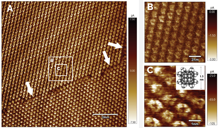
Constant height STM current images of the 2D lattice of NiOEP on HOPG
(A) 50 nm survey scan showing the NiOEP grain boundary (white arrows), zoom regions, and moiré pattern imaged with a 6.4 pA setpoint. (B) Zoomed 10 nm region imaged at 300 fA setpoint. (C) Zoomed 5 nm region showing sub-nm molecular resolution imaged with a 60 pA setpoint. Inset: the CPK molecular model of NiOEP.

© Oxford Instruments 2026