AFM Systems
AFM Accessories
Learning
Contact Us
 Part of the Oxford Instruments Group

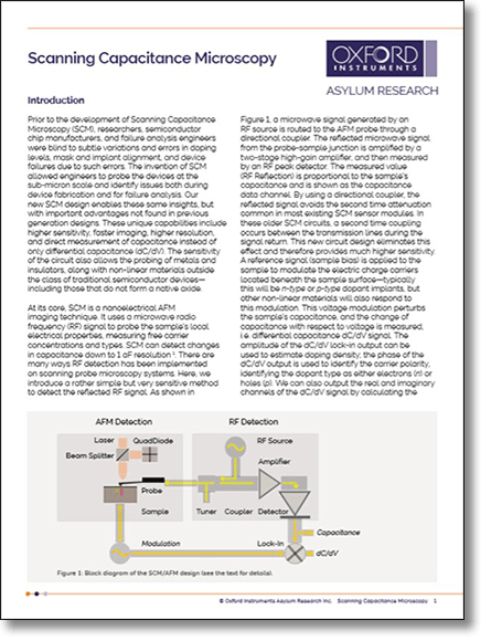
Scanning Capacitance Microscopy (SCM) is a powerful imaging mode that allows researchers and engineers to directly visualize small variations and errors in both mask and implant alignment and dopant levels and to understand failures that arise from these issues.
The recently released SCM module for Asylum Research Cypher and Jupiter atomic force microscopes enables these same insights but offers significant advantages compared to previous generation designs, including higher sensitivity, higher resolution, faster imaging, and the ability to directly measure capacitance and not just differential capacitance (dC/dV). This application note describes:
The application note will be of interest to:
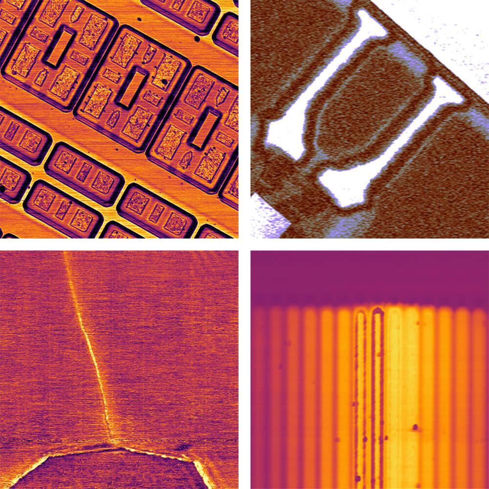
(Top-left) Asylum's SCM module can directly measure capacitance, not just dC/dV. Here, we show a SRAM sample commonly used as a SCM test sample.
(Top-right) The SCM module can also capture images much faster than others. This image was scanned at 8 Hz, about 8-16× faster than typical SCM.
(Bottom-right) Unlike dC/dV amplitude data, the capacitance data is linearly correlated with dopant levels in this dopant staircase standard sample.
(Bottom-left) Higher sensitivity allows the Asylum SCM module to image samples beyond traditional semiconductors, here a carbon nanotube.

© Oxford Instruments 2026