AFM Systems
AFM Accessories
Learning
Contact Us
 Part of the Oxford Instruments Group

Oxford Instruments Asylum Research is pleased to sponsor an online virtual symposium on Applications of Atomic Force Microscopy in 2D Materials Research. The symposium will feature a panel of leading researchers who will each describe the role of atomic force microscopy in their research projects and share recent results. Individual Q&A sessions after each presentation and a panel discussion at the conclusion will provide ample time for attendees to address questions to the speakers.
Wednesday, September 8th, 2021 from 7-9 am PDT (14:00-16:00 UTC)
Dr. Laura Fumagalli
University of Manchester
Dr. Jonathan Bradford
University of Nottingham
Dr. Vinod K. Sangwan
Northwestern University

Laura Fumagalli is Reader in Condensed Matter Physics at the Department of Physics & Astronomy and staff researcher of the National Graphene Institute. She received her M.S. in Electronic Engineering in 2002 (Polytechnic University of Milan - Italy and École Superior d’Electricité - France) and her PhD in Information Technology in 2006 with a doctoral thesis on low-noise wide-bandwidth amplifiers at the Department of Electronics of Polytechnic University of Milan. She then worked at the Department of Electronics of the University of Barcelona (Spain) as post-doctoral researcher (2006-2010) and lecturer (2010-2014), developing novel instrumentation and methods that measure the dielectric properties of matter on the atomic scale using a scanning probe, referred to as Scanning Dielectric Microscopy (SDM). She joined the Condensed Matter Physics group of the University of Manchester (UK) in 2015. She was awarded the Ramon y Cajal fellowship by the Spanish Ministry of Education and Science in 2014 and the ERC Consolidator grant "Two-dimensional liquid-cell dielectric microscopy (Liquid2DM)" by the European Research Council in 2018. She currently sits in the scanning probe microscopy committee of the Royal Microscopical Society. Her research focuses on the study of electric and dielectric properties of bio and non-bio materials on the nanoscale.
In this talk, after briefly reviewing scanning dielectric microscopy, a set of scanning probe microscopy methods that we developed to probe dielectric properties on the atomic scale [1-3], I will present our recent studies applied to the case of van der Waals (vdW) heterostructures [4-6]. First, we succeeded to measure the dielectric constant of few water layers confined into atomically flat nanoslits made of graphite and hexagonal boron nitride (hBN) [4]. Our work revealed the presence of an electrically dead water layer with vanishingly small polarization at the solid/liquid interface, providing much-needed feedback for theories describing interfacial water and water-mediated surface interactions. We then focused on the properties of hBN heterostructures. Our experiments revealed that monolayer hBN is piezoelectric, while we found no piezoelectricity in bilayer and bulk hBN [5]. Our experiments also revealed that marginally twisted hBN heterostructures, two hBN crystals stacked at small twist angle, have ferroelectric-like superlattice domains [6]. These findings open up new possibilities for understanding electric polarization on the atomic scale and designing novel devices with piezoelectric and ferroelectric properties based on van der Waals heterostructures and liquids confined inside.
References
[1] L. Fumagalli et al. Appl. Phys. Lett. 91, 243110 (2007)
[2] L. Fumagalli et al. Nature Mater. 11, 808 (2012)
[3] G. Gramse et al. Appl. Phys. Lett. 101, 213108 (2012)
[4] L. Fumagalli et al. Science 360, 1339 (2018)
[5] P. Ares et al. Adv. Mater. 32, 1905504 (2020)
[6] C. R. Woods et al. Nat. Commun. 12, 347 (2021)

Jonathan Bradford is a Postdoctoral Research Fellow in Professor Peter Beton’s group at the University of Nottingham, specialising in bottom-up growth of 2D materials and their characterisation using scanning probe microscopy and photoemission spectroscopy. He received a B. Applied Science (Physics) & B. Mathematics from the Queensland University of Technology (Brisbane, Australia) in 2014 before completing his PhD studying the growth of 2D material heterostructures (hBN, MoS2, WS2) based on epitaxial graphene/SiC in 2019. Following this, Jonathan joined the School of Physics and Astronomy at the University of Nottingham in 2019 working on the growth of graphene and hexagonal boron nitride heterostructures by high temperature molecular beam epitaxy.
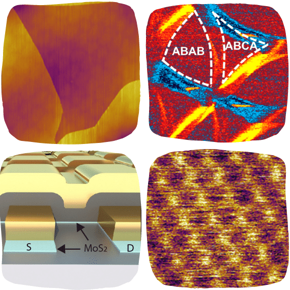
Integration of graphene and hexagonal boron nitride (hBN) in van der Waals and lateral heterostructures has led to the emergence of a range of quantum effects and has provided a route to broadly engineer the material properties for diverse applications in nanoelectronics. We have demonstrated van der Waals epitaxial growth of graphene on hBN using high temperature molecular beam epitaxy (MBE). This approach uniquely enables the growth of intrinsically highly strained graphene layers which exhibit a moiré superlattice with a periodicity depending on the tensile strain and can be lattice matched to the hBN substrate at sufficiently high growth temperatures. We have also utilized plasma-assisted MBE to grow epitaxial hBN layers on HOPG which acts as a tunnel barrier comparable to exfoliated hBN, and exhibits deep UV luminescence. Finally, we use MBE to form lateral heterostructures of graphene and hBN wherein a graphene nanoribbon is passivated by hBN. Comprehensive studies of the graphene nanoribbons by atomic force and scanning tunnelling microscopies (AFM & STM) reveals that graphene nanoribbons grow conformally from the edges of hBN domains with a controllable width that is highly uniform across the surface. Lattice and atomic resolution imaging of the hBN/graphene interface indicates that the graphene nanoribbons retain the lattice orientation of the free hBN edge, enabling selective growth of armchair and zigzag heterointerfaces.
*Note: Professor Beton became unable to participate in the symposium and requested that Dr. Bradford present their work.

Dr. Vinod K. Sangwan is currently a Research Assistant Professor in the Department of Materials Science and Engineering at Northwestern University. He did a B. Tech. in Engineering Physics at Indian Institute of Technology Mumbai and later, a Ph.D. in Physics at University of Maryland College Park. His research at Northwestern University intersects multiple disciplines of applied physics, electrical engineering, and physical chemistry. Recently, he has been actively pursuing research in hardware neuromorphic computing, optoelectronics, photovoltaics, and topological quantum materials. In the context of this talk, Dr. Sangwan is developing novel device concepts towards tunable nanosystems that efficiently emulate bio-realistic behavior in artificial synapses and neurons. He has published more than 80 journal papers, has 10 granted and pending patents, and has mentored two dozen graduate and undergraduate students.
Hardware implementation for neuromorphic computing aims to overcome the von Neumann bottleneck by co-locating memory and logic. In this context, emerging non-volatile memories are being explored extensively for artificial synapses and spiking neurons. For example, neuromorphic devices based on low-dimensional nanomaterials have begun to show promise due to their controlled chemical composition, unique architectures, and compatibility with ultimate scaling and speed limits. Furthermore, low-dimensional materials enable enhanced electrostatic control, thus allowing functions that better mimic a biological neuron. Scanning probe microscopy is a core technique for characterizing these nanoscale device applications.
In this talk, I will discuss recent advances in the development of artificial synapses and neurons based on 2D semiconductors and mixed-dimensional van der Waals heterojunctions. In particular, dual-gated memtransistors based on polycrystalline MoS2 show novel synaptic responses in crossbar arrays. The non-volatile memory states of these devices are tuned by both biasing history and the field-effect from the two gate terminals. The dual gates allow independent addressing of nodes in the crossbar by minimizing sneak currents in addition to facilitating tunability of synaptic weight update rules that resulted in a 94% recognition rate of hand-written digits. In the second part, I will discuss a dual-gated, self-aligned, mixed-dimensional p-n heterojunctions Gaussian heterojunction transistor that realizes the functionality of an integrate-and-fire neuron and other spiking behaviors. I will emphasize the role of atomic force microscopy in characterizing atomic defects and grain boundaries that enable underlying switching mechanisms in these devices.

© Oxford Instruments 2026