Tags: AFM, Atomic Force Microscopy, conductive AFM (CAFM), Kelvin probe force microscopy (KPFM), Scanning Probe Microscopy, SPM
U. S. researchers demonstrated a solution-processing technique for molecular-doped MAPbI3 solar cells. The approach simplifies device architecture and reduces fabrication costs by removing the need for a separate hole transport layer. AFM electrical characterization confirmed the method yielded high-efficiency devices.
 Halide perovskite materials such as MAPbI3 (methylammonium lead iodide) show great promise for next-generation solar cells due to their high efficiencies and relative ease of fabrication. At this point, successful commercialization requires new processes for low-cost, high-throughput manufacturing. A key issue is the hole transport layer (HTL) of current designs, which increases cost and hinders scale-up.
Toward this end, researchers at the University of North Carolina and the University of Nebraska–Lincoln demonstrated a molecular-doping strategy for preparing MAPbI3 films via a doctor-blade process. Doping with F4TCNQ (2,3,5,6-tetrafluoro-7,7,8,8-tetracyanoquinodimethane) molecules eliminated the need for HTLs while yielding devices with power conversion efficiencies (PCEs) of over 20%.
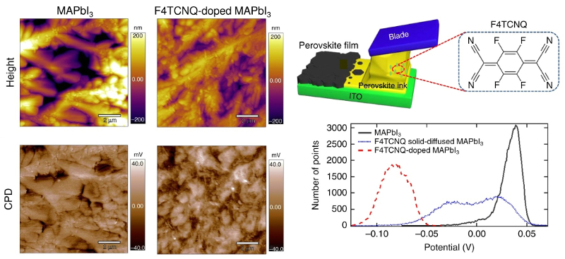
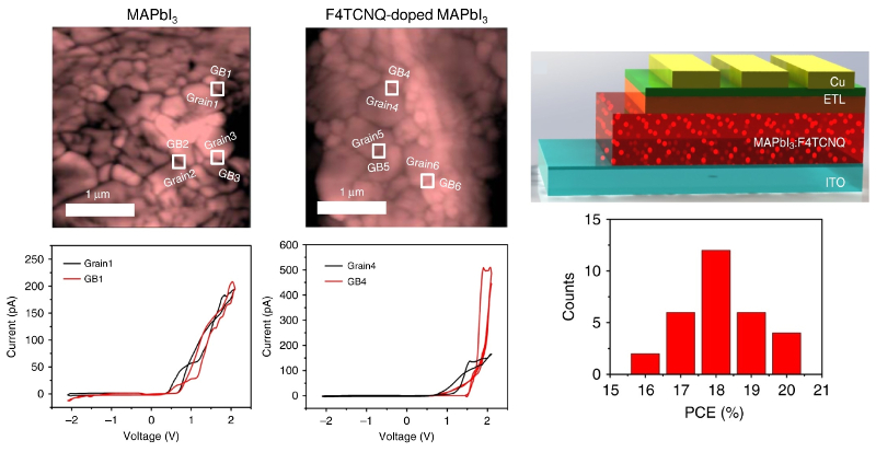 AFM characterization provided deeper insight into the electrical properties of films made with the new process. Nanoscale electrical imaging showed that F4TCNQ-doped MAPbI3 films had lower contact potential difference and thus more effective electron transport than undoped films. Moreover, AFM current measurements showed that doped films had higher conductivity, particularly near grain boundaries.
The results represent significant progress toward large-scale, cost-effective fabrication of high-performance solar cells.
Instrument used
MFP-3D
Techniques used
All nanoelectrical experiments were performed on the MFP-3D AFM using cantilevers with Pt-coated conductive tips. Images of contact potential difference (CPD) and topography were obtained simultaneously in Kelvin probe force microscopy (KPFM) mode. Besides confirming the films’ large grain structure, topography images identified precise sample locations for acquisition of current–voltage (I-V) curves using conductive AFM (CAFM) mode. The ORCA option for MFP-3D AFMs enables low-noise measurements of currents ranging from ~1 pA to 20 nA.
Citation: W. Wu, Q. Wang, Y. Fang et al., Molecular doping enabled scalable blading of efficient hole-transport-layer-free perovskite solar cells. Nat. Commun. 9, 1625 (2018). https://doi.org/10.1038/s41467-018-04028-8
Note: The original article featured above was published as Open Access under a Creative Commons license. The data shown here is reused under fair use of the original article, which can be accessed through the article link above.

