Tags: AFM, Atomic Force Microscopy, electrostatic force microscopy (EFM), Scanning Probe Microscopy, SPM, tapping mode
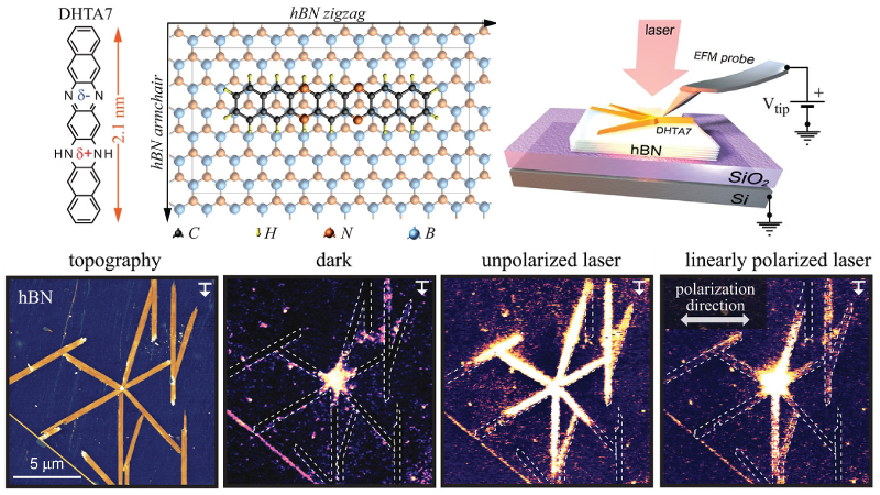
French and Austrian researchers used light to control the electrical conductivity of self-assembled organic networks on hexagonal boron nitride (hBN). AFM nanoelectrical images showed that charge propagation could be turned on and off, and even directionally guided, by illuminating the system with polarized laser light.
Layering 2D materials to create van der Waals heterostructures holds enormous potential for next-generation applications in electronics, optics, and sensing. This potential could be further expanded by incorporating organic molecules, which offer capabilities that inorganic materials cannot match.
A team of researchers at the University of Leoben, University of Graz, and Aix-Marseille University explored these ideas with the organic semiconductor dihydrotetraazaheptacene (DHTA7). They used self-assembly techniques to form networks of quasi-1D DHTA7 crystallites on insulating hBN.
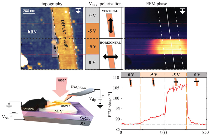
Combined with modeling, AFM nanoelectrical characterization of the networks showed that the electrical conductivity increased by more than 100× when the system was externally illuminated, enabling charge propagation. Moreover, the optical anisotropy of the nanoneedles made it possible to steer the propagation direction by adjusting the light polarization angle.
The results suggest a strategy for creating “light gates” to control electrical conductivity in organic nanostructures and demonstrate a powerful way to extend the applicability of 2D materials.
Instrument used
MFP-3D
Technique used
AFM images were acquired in electrostatic force microscopy (EFM) mode on an MFP-3D AFM. On Asylum Research AFMs, EFM is performed using a two-pass approach. In the first pass, topography is acquired in tapping mode. In the second ‘nap’ pass, this topography data allows the tip to retrace the scan line at a constant, user-defined height above the surface. Separating the tip and sample enhances sensitivity to long-range electrostatic forces, while maintaining constant height minimizes effects from other interactions such as van der Waals forces. The EFM images shown represent the phase of the oscillating cantilever during the nap pass.
Citation: A. Matković, J. Genser, M. Kratzer et al., Light-assisted charge propagation in networks of organic semiconductor crystallites on hexagonal boron nitride. Adv. Funct. Mater. 29, 1903816 (2019). https://doi.org/10.1002/adfm.201903816
Note: The original article featured above was published as Open Access under a Creative Commons license. The data shown here is reused under fair use of the original article, which can be accessed through the article link above.

