AFM Systems
AFM Accessories
Learning
Contact Us
 Part of the Oxford Instruments Group

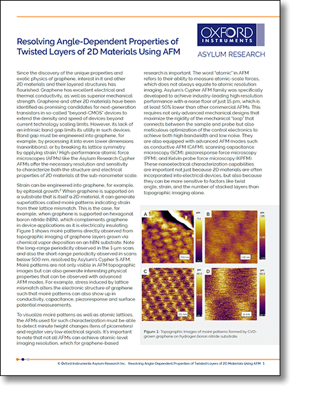
Graphene and other 2D materials may be promising candidates for constructing “beyond-CMOS” devices that enable higher density and speed than what current technology allows. It has been found that layering these materials with a slight twist angle can create a band gap in graphene, which lacks an intrinsic band gap, or tune the band gap in materials like transition metal dichalcogenides (TMDs). Characterizing these effects with atomic force microscopy requires ultra-high resolution imaging of structure and high sensitivity measurement of electrical properties. This new application note presents results from three recent publications that demonstrate how Asylum Research AFMs are being used to characterize angle-dependent properties in twisted superlattices in 2D materials.
Download the application note to learn:

© Oxford Instruments 2026