AFM Systems
AFM Accessories
Learning
Contact Us
 Part of the Oxford Instruments Group

Atomic Force Microscopy, or AFM, is a high resolution form of scanning probe microscopy that employs a sharp tip in a raster motion to measure and visualize materials at the atomic and nano scales. This overview will serve as an introduction to atomic force microscopy.
Microscopes are tools that help us see what you cannot see with your naked eye, from ancient Greek “mikrós” small and “skopeîn” to look. AFM uses a variety of techniques, also known as measurement modes, to analyze samples at a scale ranging from below a nanometer (<1 nm) (0.5 nm is the average size of an atom) up to 1 micrometer (also known as a micron). To get a feel for just how small the nano and atomic scales are, picture this - A tennis ball is to Earth as an atom is to a tennis ball:

AFM gathers information by ‘feeling’ a surface, much like a finger does but at a much smaller scale. It uses a tiny probe, with a very sharp tip, to sense small variations in force. This simple but clever idea was invented in the early 1980s and won a Nobel prize soon after in 1986.
Though most frequently used to visualize small-scale structure, AFM is also valuable for measuring local electrical, mechanical, and other material properties. Moreover, it is suitable for a wide range of materials including electrically conductive and insulating, transparent and opaque, soft and stiff, and more.
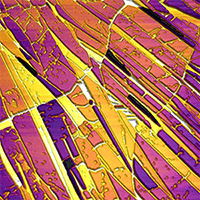
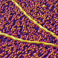
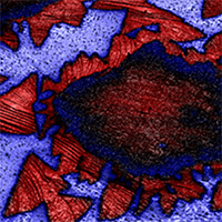
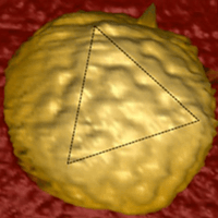
As a result, AFM has become a ‘go-to’ tool in applications across the entire R&D spectrum—everything from basic research in molecular and cell biology, bottom-up assembly, and 2D materials to industrial work in microelectronics, plastics and rubbers, and energy storage and energy generation devices. The application fields below illustrate the power and versatility of AFM (click on an AFM image below for more information).
These resources describe how AFM is used for specific applications:
AFM Applications in Polymer Science & Engineering white paper
AFM Characterization of 2D Materials white paper
AFM in Food Research white paper
Advancing Virology Research with High-Resolution AFM Imaging white paper
AFM Characterization of Emerging Photovoltaics webinar
AFM Techniques for Thin Film Analysis webinar
AFM measurements are done with an instrument called the atomic force microscope, or AFM. An AFM has three subsystems that separately perform:
1) Sensing, 2) Detecting, and 3) Positioning
-- plus controller electronics that coordinate these functions.
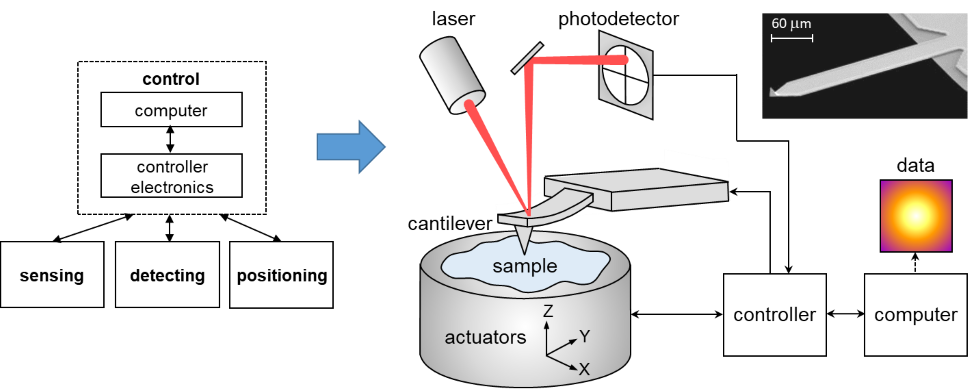
The AFM sensor is called a cantilever and has a small, sharp tip near the free end. When sufficiently close to the sample, the tip is affected by forces at the sample surface. This causes the tip to move, which in turn causes the entire cantilever to bend. The cantilever bending, or deflection, is detected optically using a laser and photodetector (a device that converts light into an electrical signal). Positioning hardware called piezo actuators is used to change the relative position between the cantilever and the sample in three dimensions.
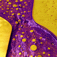
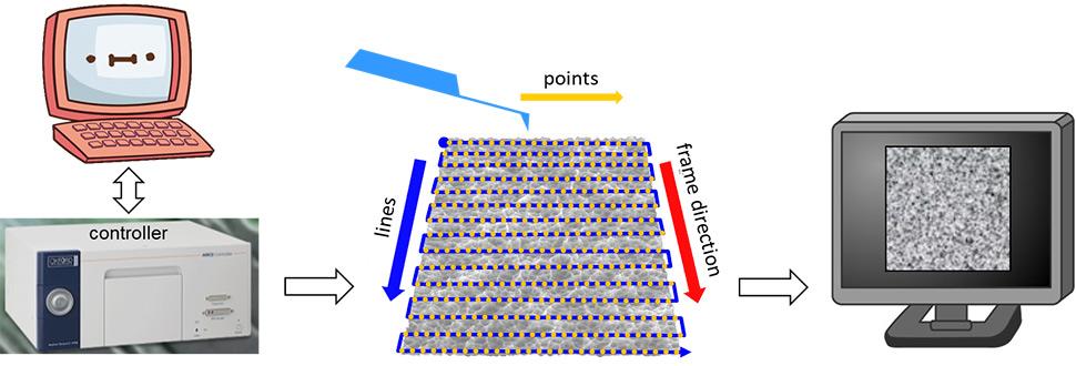
The most common type of AFM measurement is creating images of spatial variations in a signal, especially of topography (height). Images are acquired using the positioners to scan the tip across the sample and detect a 2D map of data points.
Topography images enable the visualization of many natural and synthetic small-scale structures—RNA, hemimicelles, nanoparticles, transistors, and much more. They are also invaluable for characterizing surfaces ranging from self-assembled monolayers and low-dimensional materials to films and bulk samples. Here, information on roughness, defects, amorphous and crystalline phases, and thin-film nucleation and growth can be obtained.
As well as providing 3D images, the quantitative data in topography measurements can be quickly analyzed to obtain figures of merit (e.g., average roughness Sa) for process control or other comparisons. Imaging can furthermore be performed under a variety of environmental conditions and scan speeds, as shown in the examples below. Other tools such as scanning electron microscopy (SEM), and profilometry are often used for these types of measurements as well, although none offer measurements with as much detail as AFM. Learn more about the differences between surface roughness measurement tools.
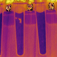
AFM force-sensing concepts also enable the measurements of local physical properties including those of electrical, mechanical, functional, and tribological nature. These measurements often provide valuable information that cannot be obtained by topography imaging alone.
For example, functional properties—electrical, electromechanical, and related behavior—impact applications ranging from solar cells to nonvolatile memory and data storage. And as devices shrink, these properties must be evaluated on smaller and smaller length scales. Several AFM modes have been developed to interrogate functional behavior on the nanoscale by sensing electrostatic, magnetic, and other tip-sample interactions. The information these modes provide can help assess uniformity, identify defects, and otherwise assure quality. In addition, it often complements and enriches data from probe stations, which test an entire device.
In other applications, mechanical and tribological properties are paramount for their role in performance and reliability. The AFM’s sensitivity to low forces enables mechanical measurements with much higher vertical and lateral resolution than otherwise possible.
Force curves are the classic way to make quantitative nanomechanical measurements. They are best suited to soft biological and polymeric materials, and can even measure bond rupture strengths in a single molecule. Force curves are acquired by bringing the tip into and back out of contact with the sample at a fixed position. A 2D array of force curves is called a force map or force volume and yields multiple images of different properties (elastic modulus, adhesion, etc.).
However, mechanical characterization of stiffer materials—up to graphene and diamond—is important for many types of advanced technology. Several AFM nanomechanical modes have been created to meet such needs. Involving a range of operating approaches, these modes can offer advantages over force curve methods such as much faster scanning and measurement of viscoelastic response.
Additional resources:
AFM Tools for Nanoscale Electrical Characterization white paper
Introduction to Piezoresponse Force Microscopy (PFM) webinar
Scanning Capacitance Microscopy white paper
Nanotribology with the AFM white paper
In just a few decades, AFM has bloomed from a Nobel prize-winning invention to an essential tool for surface analysis. Though best known for imaging nanoscale structure, it can also evaluate many physical properties on small scales. Recent instrumentation advancements such as higher spatial resolution, faster imaging rates, and enhanced environmental options make AFM more valuable than ever before. Future refinements that further extend these capabilities will ensure that AFM keeps pace with the demands of science and technology.

© Oxford Instruments 2026