Tags: AFM, Atomic Force Microscopy, conductive AFM (CAFM), piezoresponse force microscopy (PFM), Scanning Probe Microscopy, SPM
Researchers investigated reversible polarization switching in a self-assembled array of BFO nanoislands. Characterization with electrical and electromechanical AFM showed the system created a stable arrangement of confined, charged domain walls whose conductance could be varied by 1000x.
Charged domain walls (DWs) in ferroelectric materials represent a confined conduction pathway that could enable nonvolatile memory with ultralow power consumption. However, achieving the necessary control of DW location and conductance during polarization switching has remained elusive.
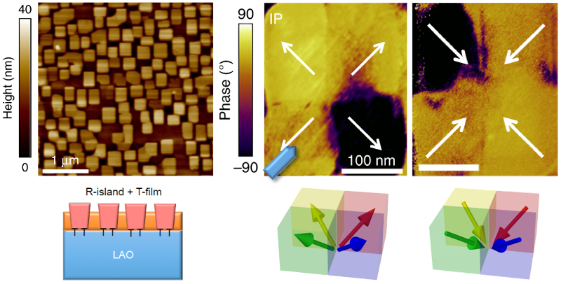
Researchers at Tsinghua University and other Chinese universities explored this topic by investigating controlled polarization switching in bismuth ferrite (BiFeO3 or BFO). Samples contained self-assembled arrays of rhombohedrally distorted (R-phase) BFO nanoislands embedded in a tetragonally distorted (T-phase) BFO film on LaAlO3 (LAO).
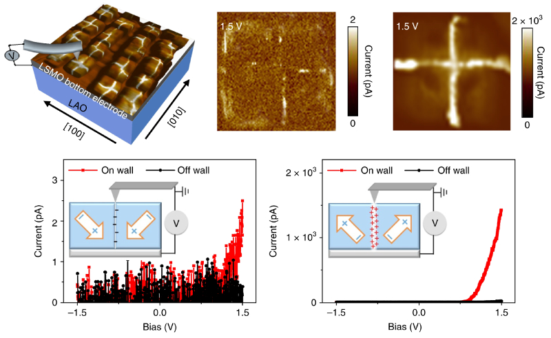
AFM measurements of current and local electromechanical response provided nanoscale information on charge conductance and polarization behavior. They showed the system had spatially confined DWs in a cross-shaped pattern with two stable domain configurations. Reversible switching between the two polarization states changed the DW conductance by more than 1000x.
Switching between high and low conductance was demonstrated for over 100 cycles, while the measured current was stable for several months. With this kind of repeatability and stability, the results could enable commercial-scale manufacturing of new ferroelectric-based nanodevices.
Instrument used
MFP-3D Infinity with the ORCA conductive AFM option
Techniques used
Current images and current-voltage (I-V) curves were acquired in conductive AFM (CAFM) mode on the MFP-3D Infinity AFM using the ORCA probe holder and a Pt/Ir-coated tip as the top electrode. As the above graphs indicate, the ORCA module enables low-noise measurements over more than four orders of magnitude (~1 pA to 20 nA). The Infinity was also used to measure local electromechanical behavior with piezoresponse force microscopy (PFM) mode. PFM images of both in-plane (IP) and out-of-plane phase were acquired at several different in-plane rotation angles for detailed reconstruction of the 3D domain structures. Together, these experiments illustrate the versatility and high performance of Infinity AFMs.
Citation: J. Ma, J. Ma, Q. Zhang et al., Controllable conductive readout in self-assembled, topologically confined ferroelectric domain walls. Nat. Nanotechnol. 13, 947 (2018).
Note: The data shown here are reused under fair use from the original article, which can be accessed through the article link above.

